SIGMA_Poster_2019

Nova Série de Transdutores de efeito Hall com desempenho Fluxgate

Série LES-LESR-LKSR-LPSR-LXS-LXSR


A nova série possui tecnologia de efeito hall de loop fechado, porém, devido aos estudos realizados pelo setor de desenvolvimento da LEM, estes novos transdutores alcançaram a performance de precisão e medição da tecnologia Fluxgate, assim destacando-se de seus concorrentes e as séries de tecnologia semelhante da própria LEM.

Características:

– Feito sob a patente ASIC LEM de efeito Hall para alto desempenho em loop fechado.

– Diversas opções de correntes nominais, de 1,5 a 50 A nominal.

-Compatíveis com as séries anteriores: LTS, LTSR, CAS, CASR e CKSR.

– 22 modelos com várias opções de: referência, base, janela ou PCB, detecção de sobre corrente (modelo LPSR).

– Drift do offset  reduzido em 4 ppm/K.

Quadro de Comparação:


Série CAS-CASR- CKSR: https://www.amds4.com.br/series/1/65/1/CAS—CASR—CKSR

Série LTS-LTSR: https://www.amds4.com.br/series/1/26/1/LTS—LTSR—LTSP

Série LES-LESR-LKSR-LPSR-LXS-LXSR: https://www.amds4.com.br/series/1/53/1/LES—LESR—LKSR—LPSR—LXS—LXSR

AMDS4-Lem-evento

AMDS4 e LEM participam da Feira FIEE Smart Future 2019

Entre os dias 23 a 26 de Julho, a AMDS4 junto com a LEM participaram da Feira FIEE Smart Future 2019.

Essa feira ofereceu acesso às tendências das tecnologias disruptivas que estão transformando a indústria através de conteúdo técnico e exclusivo, debates, demonstrações de aplicações industriais e muitas oportunidades de negócios para profissionais dos setores elétrica, eletrônica, energia, automação e conectividade.

A AMDS4 teve a oportunidade de mostrar suas novas tecnologias, tendências e produtos que trarão novas soluções para os seus negócios!
Quer conhecer um pouco mais sobre nossa empresa e produtos? Entre em contato conosco através do e-mail amds4@amds4.com.br ou pelo telefone: 19 3806-1950 / 19 3806-8509


img-08

FLUXGATE TECHNOLOGY AND THE NEW HIGH ACCURACY CURRENT TRANSDUCER (IN 2000)


Technology innovations take fluxgate current transducers to previously unattainable performance levels.


The use of fluxgate technology in transducers for precise current measurement is well-known. In order to improve performance beyond that of existing sensors new ideas are needed. This article starts with a short overview of fluxgate-based current transducers, and then it shows how applying innovations to this architecture has allowed the development of a new family of transducers. Several related improvements must be made together, and the result is a compact transducer which maintains its accuracy over a wider temperature range and has a reduced noise level. The improved performance parameters and some key results of the product characterization will be presented.


Introduction to fluxgate current transducers.


The fluxgate current transducers described in this article are closed loop devices in which the magnetic field created in a magnetic circuit by the measured or primary current, IP, is exactly cancelled by a secondary or compensation current, Icomp, passed in a coil of Ncomp turns around the same magnetic circuit. In the general case where the primary current may have Np turns, IP is simply given by:


IP = Icomp x Ncomp / Np


The zero-field condition is detected by a fluxgate, which consists of a coil wound around a ferromagnetic core that saturates in the presence of a magnetic field. The inductance of the coil reduces when the core saturates. If a symmetrical square-wave voltage drives the fluxgate the rate of change of its current will increase when it saturates but the current waveform will be symmetrical unless a magnetic field due to the primary current is additionally applied, in which case the waveform will be asymmetric.


Figure 1. (a) Fluxgate drive waveform; (b,c) Fluxgate current in the absence and presence of an external magnetic field.


This is shown in figure 1: trace (a) shows a square applied voltage waveform, which has only odd harmonics of the fundamental frequency; trace (b) is the symmetrical current waveform obtained when the external magnetic field is zero; it also has only odd harmonics; trace (c) shows an asymmetric waveform when the external field is not zero; this waveform contains even harmonics and a DC component.


Figure 2 shows the operating principle of a current transducer using this principle. The square wave voltage is applied to the fluxgate with the H-Bridge; its current is converted to a voltage by resistance R, and its symmetry is measured by a signal treatment such as detecting the second harmonic of this waveform. The loop is completed by driving the compensation current with the Class AB amplifier such that this second harmonic is zero. Icomp is converted to a voltage by Rm.


Figure 2. Operating principle of a fluxgate transducer.


Note that the fluxgate system covers the DC and low frequency range of the primary current; for higher frequencies the current transformer effect is used directly, as well as other techniques described later.


Advantages and limitations of fluxgate current transducers.


The fluxgate is a passive element which is driven symmetrically; together with the use of the second harmonic to detect zero field this gives a system whose offset – and, more important, whose offset drift – is low, being principally constrained by the electronics of the feedback system. The turns ratio Ncomp / Np is exactly known, so the transducer is very accurate and stable. It operates at zero magnetic field provided that the loop gain is high enough, which gives a system having excellent linearity. The transformer effect allows for a good response at high frequencies. Unlike a Hall-cell based transducer there is no sensing element with a high resistance so the white noise is low.


However there are some limitations.


The voltage drive which excites the fluxgate may couple into the secondary current and add an unwanted signal, or ripple, at the excitation frequency. This can be overcome by driving a dummy fluxgate in anti-phase to the one used in the measurement loop, though the effectiveness of this is limited by the fluxgate matching.


In general the fluxgate loop will not function up to the frequency at which the transformer effect takes over. This frequency gap must be filled – for example, by a pick-up coil whose output voltage is proportional to the rate of change of the primary current; after integration this signal is summed with the output of the second harmonic detector and used to drive the secondary current.


Figure 3 shows a more complete version of the transducer of figure 2, including the components which overcome these two limitations.


Figure 3. A complete fluxgate transducer including the blocks needed to overcome the limitations inherent to the system.


Note however that the electronics in the control loop is quite complex and if it is implemented in the analog domain there are many blocks which have the potential to contribute offset, noise from the supplies, and so on. In some transducers this electronics is physically separate from the magnetic components at the heart of the system; an example is shown in figure 4.


Figure 4: A 2000 A transducer (ITZ 2000) of an earlier generation which is in two parts, one for the measuring head and one for the electronics.


In certain situations, such as when IP exceeds the measurement range, the fluxgate may always be saturated which gives a ‘false zero second harmonic’ condition. The loop which generated Icomp then has no gain, since changing Icomp gives no change in the second harmonic measurement. This condition needs to be detected and corrected.


New innovations improve performance.


In the new IN 2000 current transducer from LEM the improvements come from a higher level of integration, performing a maximum of signal processing in the digital domain and a new approach to the architecture of ripple cancellation at the fluxgate drive frequency. The benefit of combining these three innovations is more than the sum of the benefit from each one.


Integration and digital signal processing: A key element of the IN 2000 is the use of a high performance Digital Signal Processor (DSP) in the feedback loop. This allows signal processing to be done in the digital domain which means that after the ADC there is complete immunity to temperature effects, interference and supply voltage variation. In particular, offset and offset drift are improved. There is a flash memory in the DSP, allowing the storage of some calibration parameters whose value may be adjusted for each different transducer. These features come without any increase in the physical size of the electronics.


Architecture: The DSP is used in two ways to reduce the interference or ripple from the fluxgate driving signal at a fixed frequency of 16 kHz. Instead of simply switching the fluxgate voltage between positive and negative values as shown in figure 1a, the drive waveform is shaped in such a way that the higher frequency harmonics are reduced. The remaining interference is eliminated by driving a ‘ripple compensation coil’ whose amplitude and phase are adjusted during the calibration of each transducer. The needed ripple compensation is kept constant over all operating conditions with a local loop which forces the source of the ripple –the fluxgate drive – to remain constant, so the compensation signal is always effective. Some transducers from earlier generations allow the fluxgate excitation frequency to vary in order that its current amplitude remains constant. However a varying frequency in a system may give unpredictable effects and the fixed frequency of the IN 2000 is generally preferred.


Figure 5 shows the complete IN 2000 system, including the new improvements. Their combined enhancements result in a transducer with very high accuracy and low noise, and it has these over a wide temperature range. After calibration the remaining peak-to-peak ripple is less than 50 ppm, relative to the full scale transducer output, over the full -40 OC to 85 OC operating temperature range.


Figure 5. The complete IN 2000 transducer system.


This article has described a 2000 Amp transducer, but it will be one of a family covering a range of different primary currents.


Figure 6 shows a comparison of the ripple at the fluxgate drive frequency at the transducer output. Two traces are shown to demonstrate the difference between the IN 2000 transducer and a 2000 Amp transducer of the previous generation: for the IN 2000 the ripple is hidden in the thermal noise.


Figure 6: The ripple before calibration of the compensation circuit (red trace) is comparable with the spikes of a transducer of the previous generation (blue trace); after calibration the ripple disappears into the noise at the output (green trace).


Two conditions may cause the fluxgate to be always saturated: a non-zero primary current when the transducer is powered up and a primary current which exceeds the transducer range by more than 10%. When this overload situation is detected Icomp is swept continuously between the extremes of its measuring range. In this way when Ip is again in the allowed range the fluxgate is certain to de-saturate and normal operation of the feedback loop to set a zero magnetic field at the fluxgate resumes. Saturation of the fluxgate is recognized by detecting that its current has increased.


As well as reacting to the overload condition described above, the IN 2000 is self-protected by a routine in the software that checks external and internal supply voltages. When any fault is detected the IN 2000 gives a status output on a dedicated connector pin so that the user knows that an action is needed to return to the conditions in which the measurement accuracy is guaranteed.


A 200-turn test winding is provided so that the transducer function can be checked using a current of 1 Amps without interfering with its installation in systems where access is difficult.


An important feature of the IN 2000 is its ability to operate over a wide temperature range. For this reason thermal simulations were done to ensure that there were no unexpected hotspots in the transducer. An example is shown in figure 7.


Figure 7. Thermal simulation in an ambient of 85 OC with a 2000 Amp DC primary current.


The complete transducer is shown in figure 8. The housing is metallic to give best shielding from external sources of interference. EMC immunity is further improved by situating the fluxgate inside the primary magnetic circuit.


Figure 8: The IN 2000 transducer


Table of key performance parameters.


The values of some important specification parameters of the IN 2000 are shown in Table 1.


Parameter Symbol Unit Maximum Value; -40 OC to 85 OC
Supply voltage UC Volts +/- 15, +/- 5%
Nominal current measuring range IPN A rms +/-2000 (IN 2000 transducer); AC and DC
Total current measuring range IPM A +/- 3000 Amps
Number of secondary turns Ncomp 2000
Output RMS noise up to 10 Hz, 10 kHz, 160 kHz Ino ppm 0.1, 4, 10 respectively
Output peak-to-peak ripple at 16 kHz Ino pp ppm 50
Offset at output IOE ppm +/- 10
Temperature coefficient of IOE TCIOE ppm/K 0.1
Linearity error over total measuring range eL ppm < 3
Step response time to 90% of IPN tr ms < 1
Frequency bandwidth (-3dB) BW kHz 140

Table 1: Some performance parameters. All values expressed as ppm are relative to the total current measuring range.


Characterization results.


An extensive characterization of the IN 2000 has been performed over the full temperature range. As an example, figure 9 shows the accuracy of a population of parts both at -40 OC and at 85 OC.


Figure 9. Characterization of the IN 2000 thermal drift compared with 25 OC at cold and hot extremes of temperature.


Conclusion


In general the validation of apparatus and equipment is made by certified laboratories using high-performance test benches supported by high-technology measuring devices including extremely accurate current transducers. These must therefore maintain their accuracy over the full temperature range of the equipment tested, for example, in automotive tests benches.

Performance which is needed for test equipment is also desirable for traditional industrial applications which are more and more demanding in high-performance applications such as medical equipment (e.g. MRI, proton therapy etc.), precision motor controllers and metering.

The IN 2000 transducer represents a new step forward in the performance which may be obtained from fluxgate transducers. Its high accuracy and low noise, both maintained over a wide temperature range, together with its compact physical size, will increase the breadth of applications for which this type of current transducer is the optimum choice.

img-capa-artigo-amds4-lower-size

Come discover more about the new miniature sensor – GO Series

A New Family of Miniature, Fast and Accurate Transducers for Isolated Current Measurement


David Jobling; David Barbagallo; Julien Feignon

LEM International SA

Plan-les-Ouates, Geneva, Switzerland


Abstract:


The design of isolated current transducers has been continuously driven by cost and size reduction. Continuing this trend, a new family of transducers needing no magnetic circuit has been introduced in standard small-outline integrated circuit packages. Careful design results in their accuracy being similar to those of conventional transducers with only a modest reduction in isolation voltage. Some extra features have been added.


Introduction:


Current transducers in which isolation is required generally detect the magnetic field of the measured current; this has the additional advantage of allowing both AC and DC currents to be measured. There have been two aspects to the trend in LEM open-loop current transducers in recent years: cost and size have been continuously reduced, and by using custom proprietary CMOS ASICs as the sensing element the performance parameters such as accuracy and response time approach those of more complex closed-loop transducers (Ref 1). Usually the ASIC is placed in the air gap of a small magnetic circuit which gives noise-free amplification of the field and screening from external interference. Most of LEM’s conventional open loop transducers measure currents in the range of 10 A to 100’s of A, isolation levels are up to 8 kV and the response time from 2 us.


Some applications, particularly for motor drives, have the same need for speed but are less demanding of the current range and isolation levels while having strong pressure on price. In applications such as for example white-goods, window shutters and air-conditioning low cost and small size are particularly important. For these cases LEM has now introduced an additional family of sensors, the “GO” family, whose size is reduced even further by eliminating the magnetic circuit. Instead, the primary current is passed directly into a standard integrated circuit package where its magnetic field is measured by a new ASIC derived from that used in conventional transducers. Figure 1 shows two such examples. One is in an SOIC-8 package and the 4 secondary-side pins are for the supplies, the output voltage Vout and a reference voltage Vref. The other is in an SOIC-16 package where 8 secondary pins are available so the opportunity has been taken to provide two different Over-Current Detect (OCD) warning levels; one very fast, and the other slower but more accurate. The speed and accuracy of the GO transducers are very similar to those of a transducer with a magnetic circuit. The absence of a magnetic circuit of course means that there is zero magnetic offset.


Figure 1: The GO series transducers and their pin connections in SOIC-8 and SOIC-16 packages.


Architecture and features:


The GO transducer ASIC is derived from that used in LEM open-loop transducers which have a magnetic circuit. There is considerable production experience with this ASIC, which has allowed introduction of some extra features around the well-known signal path blocks. In this section the design of the GO transducer is described and some contrasts are made with magnetic circuit transducers.


Figure 2: Block diagram of a GO transducer in an SOIC-16 package.


Figure 2 shows a simplified block diagram of a GO transducer in a 16-pin package. Multiple Hall cells implanted in the ASIC are placed on both sides of the primary current to detect its magnetic field. Their offset, together with that of the input amplifiers, is eliminated with chopping techniques which modulate the Hall cell output to an AC signal. After amplification the Hall signal is demodulated back to its original frequency before buffering and filtering at the output. The fast response time is achieved by using a high chopping frequency and internal filters which reduce the noise bandwidth of the system.


During production each transducer is individually calibrated. Tests are done at 3 temperatures; the drifts of sensitivity and output offset are measured and corrections stored in an EEPROM memory on the ASIC; this ensures that the transducer accuracy is maintained over temperature and aging.


The ASIC is separated from the primary conductor by a series of insulating layers – an optimum separation has been chosen for the best compromise between highest isolation with a wide separation and highest magnetic field at the Hall cells with lower separation. The Hall cells on opposite sides of the primary are sensitive to fields in opposite directions so the transducer is immune to uniform magnetic fields from sources other than the measured current. The exact lateral position of the Hall cells relative to the primary is not critical, since the difference between the outputs of the cells on the opposite sides is used. In other words, the Hall cells are configured as a gradient sensor.


Figure 3: Block diagram of the Over-Current Detect (OCD) systems.


The detail of the OCD implementation is shown in figure 3. The aim is to give two different levels of warning. The first level is for currents slightly higher than expected, to warn for example that a drive current is going out of the expected range. This OCD needs to be reasonably accurate, not especially fast, and each user may want to set a different level. The relaxed speed requirement allows the input to this first OCD to be taken from the transducer output, and the level is set by user-chosen external resistors, hence its name, OCD_EXT.


The second level is intended to warn of currents which are dangerously high, due to a short circuit for example. The response time must be extremely fast, but the value and accuracy of the of the detection level are not critical. To obtain a fast response time and to allow an OCD level outside the normal linear operating range the input to the second OCD is taken before the demodulation block. Its level is set internally by storing a parameter internally in the EEPROM – so it is known as OCD_INT. The level is typically set at 3x the nominal primary current, IPN.


Figure 3 is slightly simplified: it omits the detail that ensures that both OCDs respond to both positive and negative over-currents.


Both OCDs check that the over-current condition is present for at least 1us approximately, to avoid false alarms, and both outputs, once triggered, are maintained for 10us to be sure that the condition can be detected. The outputs are open-drain, which conveniently allows OCDs from several transducers to be connected together. OCD_INT triggers in less than 2.1 us; the typical response time of OCD_EXT is 10 us.


The footprint of a GO series transducer in a 16-pin package is about 100 mm2, and in an 8-pin package it is half of this. The corresponding value for the smallest PCB-mounted transducer with a magnetic circuit is about 400 mm2. The heights are 2.5 mm and 12 mm respectively. However, for both types, in the higher current ranges some allowance must be made for dissipation of the heat generated in the transducer primary, which is greater in the GO series since the primary resistance is higher.


Key parameters and measured transducer performance


In Table 1 some of the key electrical parameters of the GO series transducers are presented. For comparison, the values of the same parameters for a small open-loop transducer with a magnetic circuit are also given – a small transducer has been chosen to give the most meaningful comparison, a larger transducer would have different parameter values.


Parameter GO transducers Magnetic circuit based transducers
 
Nominal current range 10 A – 30 A 3 A – 50 A
Supply 3.3 V or 5 V; 19 mA 3.3 V or 5 V; 19 mA
External field immunity Yes: gradient sensor Yes: magnetic circuit screen
Insulation test, 50 Hz, 1 min 3 kV 4.3 kV
Impulse test voltage, 50 us 4 kV 8 kV
Creepage, clearance distances SOIC-8: 4 mm; SOIC-16: 7 mm >8 mm
Accuracy at 25°C 1.0% 1.0%
Accuracy over 25 – 105°C 3.0% 3.4%
Primary resistance 0.7 mW 0.2 mW
Out-of-range detection Yes, 10 us response time No
Short-circuit detection Yes, 2.1 us response time Some models, 2.1 us
Response time <2.5 us <2.5 us
Offset drift (10 A model) 0.9 mA/K 0.9 mA/K
Sensitivity drift 150 ppm/K 200 ppm/K
Magnetic offset 0 0.25 A after 10x IPN
Footprint 50 – 100 mm2 400 mm2 or more
Height 2.5 mm 12 mm or more

Table 1: Comparison of key parameters of GO series and magnetic circuit based transducers.


Table 1 shows that many key electrical parameters have been inherited unchanged or slightly improved from the established sensors with a magnetic circuit, whereas others, such as size and insulation, are different, allowing the two transducer families to address quite different markets.


Figure 4: Response time measurement of a GO transducer.


Figure 4 shows a measured response time after a primary current change in 0.3 us. The compact size and absence of magnetic components in the transducer gives a response with very little overshoot and ringing.


The assertion made previously that the GO transducers are not disturbed by external magnetic field will be true if the amplified electrical output of the Hall cells from both sides is the same, since the difference between the two outputs is used. To satisfy this condition:


(i) The sensitivity of the Hall cells on both sides of the primary (and the amplifiers to which they are connected) must be the same; that is, they must be well matched;

(ii) The magnetic field must be the same on both sides of the primary; it must be uniform.


Considering point (i), because the Hall cells and the amplifiers are made with large devices, their matching is excellent. When a uniform external magnetic field is applied to a GO transducer it is almost perfectly rejected.


However, for point (ii) the magnetic fields generated by conductors placed close to the transducer are not uniform and the outputs from the two sides of the primary will not be perfectly rejected. This has been investigated for conductors placed in 4 different positions near a GO transducer; see figure 5. The worst case is position 3 in which the external conductor is aligned with the GO primary. If the external conductor carries 10 A and the measured current is also 10 A the transducer output error due to the external current will be only about 1% of the measured current even with zero distance between the external conductor and the GO. This investigation shows that with a minimum of care in the design of PCB layout, external conductors will have negligible influence on the accuracy of GO series transducers.


Figure 5: The effect of external conductors on the accuracy of a GO transducer. The error is shown when the currents in the GO primary and the external conductor are the same.


Another important consideration in miniature transducers is the effect of a sudden primary voltage change on the transducer output. This is best handled at the ASIC level. Where internal signal levels are small they are always differential, and changes in their common mode level due to an external transient have little effect. Sensitive nodes can be protected by small grounded screens on the top metal layer. Screening is used only over the small areas where it is needed. This has many advantages over large screens: the top metal layer remains available for interconnect where screens are not needed; the ASIC die is not hidden and damaged parts can be analysed, and there are no Eddy currents which would slow the response time.


Figure 6 shows the effect of a dv/dt of 5kV/us on the output of a 25 A GO (GO 25-SMS). The peak disturbance on the output is 4% of IPN and the recovery time is about 3.6 us.


Figure 6. Response of a GO transducer (GO 25-SMS) after a dv/dt disturbance.


Conclusion


This paper has introduced a new series of miniature, fast and accurate transducers for isolated measurement of AC and DC currents. Some of their electrical parameters are similar to those of transducers with magnetic circuits and others are altered. Different transducers will be suited to different applications and the addition of this series to the LEM catalogue will extend system designers’ possibilities for optimizing their systems with the most efficient cost effective means of isolated current measurement.


Reference 1: David Jobling: New open-loop current transducers with near closed-loop performance. Proceedings of the PCIM Conference, May 2014, page 222-6.

IMG-10

Why do current transducers go digital?

LEM pioneers current sensing and develops digital output transducers with a sigma-delta bit stream interface (Subtitle)

By: Pascal Maeder (Global Product Manager, Drives/Welding)

Sources: David Jobling (ASIC Development Group Manager)
Stéphane Rollier (Product & Marcom Manager)
Mathieu Béguin (Marketing Engineer)


Why do current transducers go digital?

A couple of years ago, LEM’s Sales & Marketing observed the first signs of a technological turnaround: some of the leading OEMs (Original Equipment Manufacturers) in the servo-drives and robot industry were thinking of abandoning analog interfaces on their systems.

This change was driven by the evolution of controllers: the “brains of the machines”. The controllers function fully digitally internally and generally only had A/D’s (analog-to-digital converters) on their interfaces. This is no longer the case today; the A/D’s are disappearing in new controllers and customers are now asking for current transducers with a digital output so that they can easily connect to their new micro-controllers. Another advantage of a digital interface is that it is less sensitive to electro-magnetic interference.

Defining and developing products based on a new technology is complex and long: you cannot afford to get it wrong. After a comprehensive market survey conducted in 2013 by LEM’s marketing & product management teams, the R&D department started developing a Hall-based open-loop ASIC. The analog to digital (A/D) conversion is performed by an on-board sigma-delta modulator, giving a 1-bit serial bit stream output, with a sigma-delta modulator at the output.

The first prototype transducers were delivered to “alpha customers” at the end of 2015. The initial feedback was positive and LEM presented these future products at the PCIM tradeshow 2016 in Nuremberg, where more users showed interest in using this new technology.


The products

LEM proposed a range of digital output versions of the successful HO and HLSR open-loop Hall effect current transducers. These new components are for nominal current measurements of 10, 32, 50, 80, 100, 120, 150, 200, 250 ARMS in 3 different mechanical designs (PCB and panel mounting) and provide up to 12 bit resolution with 20 kHz bandwidth. The single-bit output minimizes the connections required, enabling highly compact transducers, and the digital output allows the user to choose the filter used on the bitstream to optimize between resolution and response time, according to the application. Digital outputs are also intrinsically immune to noise in hostile environments.


Fig.1: HLSR 50-PW, the digital version of LEM’s successful HLSR 50-P transducer (analog output).


The digital interface

The transducer output is a bit stream where the density of 1’s depends on the current measured, as illustrated in figure 2.


Fig.2: The digital conversion with a ∑Δ Modulator.


The detail of the transfer function is shown in figure 3. This shows the average density of 1’s on a scale from 0 to 1, and the same output if it is filtered and represented as a 16-bit word on a scale from 0 to 65’535 (decimal). See the next section for more on filtering options. Figure 3 also shows the equivalent output from an analog sensor. As with the analog sensor the performance of the new sensor is over the range +/-IPM, corresponding to an average density of 1’s from 0.1 to 0.9.


Figure 3: Transfer function.


The digital filter is implemented by the user, see figure 4. The advantage is that the number of connections to the transducer is minimized; each user can decide the filter(s) best suited to the application and the output format can be selected to match the system requirements.


Figure 4: LEM provides a bit stream output.


Performances and filter choices

Any conversion from an analog to a digital signal involves quantization, and the error between the digital signal and the exact value of the analog signal it represents is equivalent to the addition of noise. The output from a sigma-delta modulator is more than simply a bitstream with a certain density of 1’s and 0’s; the sequence is randomized in a way that pushes the quantization noise out of band to frequencies higher than those of interest for current measurement. The user processes the bitstream in a digital filter which rejects the high frequency noise. As with any filter, compromises are made to optimize system performance: a narrow bandwidth gives lowest noise (or highest resolution) at the expense of response time, and vice versa. In the example of figure 5 the bitstream is processed twice: in a 20 kHz filter which gives a resolution of 12 bits for accurate measurement of the primary current and in a wideband filter to detect excess currents with a response time of 5μs. Additionally the transducer internal OCD (over current detect) output allows detection of short circuits with a response time of only 2.7 µs.


Figure 5: Application example with OSR and filter order influence on response time and resolution.


Bits are processed one at a time in the digital filter. Due to the modulator oversampling ratio (OSR), the digital filter output can be processed every OSR bits with no loss of information within the band of interest.

The latency of filter depends on its very nature: output is delayed by 2 x OSR x CLK period for a sinc2 whereas 3 x OSR x CLK period are needed to get the exact output after a step response with the very common sinc3 filter. The bit rate at the output of LEM’s new sensors is 10 Mb/s. The combination of OSR, filter choice and bit rate leads to the response time, the bandwidth and the effective resolution of each of the signal paths connected to the bitstream, as shown in figure 6 of the HO 150-NPW performance.


Figure 6: HO 150-NPW performances: Performances = f (OSR, SINC K FILTER, BANDWIDTH).


The resolution of the complete system including the analog part of the transducer, the sigma-delta modulator and the digital filter is limited either by the quantization noise inherent to the system or by the analog noise from the Hall cells and amplifiers. For fast response times (for example with an OSR of 16 and a sinc2 filter) the resolution is defined by the system and will be the same with any transducer. If the filter is changed to sinc3 and the OSR is increased the effective resolution is improved but will be limited to 11 – 13 bits (depending on the sensor sensitivity) by analog noise. The term “Effective” resolution is used because for system convenience the filter may output a word with a length of 16 bits or 2 x 8 bits. However only the most significant bits corresponding to the effective resolution contain useful information, the less significant bits contain noise.

Usually the digital filter output is sampled at a frequency equal to the bit rate divided by the OSR; this is referred to as decimation. With the LEM sensors if the OSR is 64 the output is updated every 6.4 us.


Physical interfaces

To transmit the bitstream LEM offers the choice between two physical interfaces. In both cases the bit rate is 10 Mb/s.


CMOS Single-ended

With the first, clock and data are provided as single-ended CMOS levels (Uc and GND). This is suitable for transmission over short distances, up to some 10’s of centimeters, after which EMC issues may become important. The maximum allowed capacitive load is 30 pF. The transducer pin allocation and timing diagram are shown in figures 7-8.


Figure 7: Single-Ended CMOS levels wiring.


Figure 8: Single-ended output (CMOS levels).


Manchester RS422

The second interface is suitable for transmission over longer distances. In this case the clock and data are combined as a Manchester coded signal. This is output on transducer pin 3 and its complement on pin 4. The differential signal thus generated is compatible with the RS422 standard. By keeping the two signal tracks physically close, EMC effects, both transmitted and received, can be kept to a low level. The pin allocation and timing diagrams are shown in figures 9-10.


Figure 9: Manchester interfaces wiring.


Figure 10: Manchester transmissions data.


Conclusion

This technological leap is not “just a new family of transducers” for LEM and the industry.

The outlook for digital output transducers is very encouraging: customer feedback shows that a significant part of the market will shift to digital interfaces, starting with the high-end servo drives. We expect more industry segments to follow this trend. Our industry is going digital and LEM is leading the way!

Figure 4: LPSR current transducer with an ASIC using the Hall effect Closed Loop technology

MAKING SINGLE-PHASE SOLAR INVERTERS SMALLER, CHEAPER & SAFER

ABSTRACT :


New technologies allow photo-voltaic (PV) inverters to switch at ever higher frequencies and consequently they are becoming much smaller and lighter. International competition and the move away from subsidies for new installations mean that there is strong pressure on their cost. The current transducers used in PV inverters must follow these trends: they must have a reduced footprint while having equivalent or improved performance at lower cost, compared to the transducers they replace. Typically PV installations use current transducers in three places. One is on the DC side, for the maximum power point tracking (MPPT) system. Two are on the AC side: first to define the parameters of the output current waveform, and secondly for safety reasons: for Residual Current Measurement (RCM) in the output caused by earth leakages, so the system may be closed down if necessary. This article shows how recently introduced LEM transducers can be used for MPPT and for AC waveform management, and then presents a new compact transducer specifically designed for RCM.


  1. INTRODUCTION


Figure 1 shows main components around an inverter in a PV system typically used in residential installations of up to approximately 20kW. Several such inverters may be combined to make the complete installation which is connected to the grid via metering apparatus.

Figure 1. An inverter system for Photo-Voltaic installations.


Figure 2. Voltages and residual currents in the PV installation


During the last decade new silicon MOSFETs have been introduced in inverters, and in future MOSFETs based on SiC and GaN will begin to replace those using silicon. This is allowing higher frequency switching which in turn means that reactive components (inductors, capacitors) of lower value, and hence smaller physical dimensions, can be used. A 2kW inverter available in 2010 and weighing over 20 kg according to the manufacturer’s datasheet has been replaced in 2016 by a model weighing less than 10 kg. In order that the current transducers used as measurement devices in a PV system continue to use a negligible part of the overall space and weight budget, their size must also reduce without any performance degradation. Similarly their cost must reduce to follow the downwards cost trend of the complete inverter system.


There are 3 LEM current transducers in figure 1, all containing custom proprietary CMOS ASICs with fully integrated Hall cells. On the DC side of the inverter there is an open-loop GO; on the AC side a closed loop LPSR for the inverter control system and at the output an LDSR, a new differential transducer for RCM also with a closed loop architecture. (For a detailed explanation of Hall effect open and closed loop transducers see Reference (1)


Figure 2 shows the voltage waveforms on the DC and AC sides of the inverter. Note that in a transformer-less system, the “DC side” does indeed have a DC voltage corresponding to the output of the photovoltaic cells between the PV+ and PV- nodes (this may be increased by a DC-DC converter) but each of the PV nodes also has an AC voltage whose peak value is similar to the peak output voltage of the AC side. If not considered at the system level this represents a serious safety hazard.


  1. CURRENT TRANSDUCERS IN THE PV INVERTER


2.1 The DC side.


Depending on the illumination intensity of the PV cells the load which maximizes the power transferred from them varies, and so the control system uses a real-time MPPT algorithm to load the cells for maximum power transfer. In the case of motorized PV panels the MPPT algorithm can also be used to obtain the optimum orientation. Since the target of the algorithm is simply to find the peak in the power transfer the accuracy requirement on the current transducer used is not demanding, and an open-loop transducer is ideal for this purpose. LEM has recently introduced the GO family of transducers (Reference (2)) which have the primary conductor integrated into a standard IC package. This gives a 70% PCB footprint reduction compared with a small transducer including a magnetic circuit. The SOIC-16 transducer is shown in figure 3. The principal specification parameters of the GO-SMS transducer in its SOIC-16 packaging are shown in Table 1.

Figure 3: GO-SMS transducer in an SOIC-16 package


Parameter GO-SMS transducers
Nominal current range (A) 10  – 30
External field immunity Yes: gradient sensor
Insulation test, 50 Hz, 1 min (kV) 3
Impulse test voltage, 50 us (kV) 4
Creepage, clearance distances (mm) 7.5
Accuracy over 25 – 105°C (%) 3.25
Primary resistance (mW)  0.75
Out-of-range detection Yes, 10 ms response time
Short-circuit detection Yes, 2.1 ms response time
Response time ms <2
Offset drift (10 A model) (mA/K) 0.94
Sensitivity drift (ppm/K) 150
Magnetic offset 0
Footprint (mm2) 100


Table 1. Main performances of the GO-SMS transducer


The accuracy of the GO transducers exceeds that which is needed for the MPPT algorithm, and they may also be used at system level for other purposes, for example by comparing the outputs of different PV panels receiving similar illumination to identify faulty panels.


2.2 The AC side.


The transducer shown after the inverter in figure 1 is a key element of the control loop which drives the inverter switches and so governs the accuracy of the current output waveform. It must have a fast response time, low noise and good linearity, and in particular the offset and its drift with temperature must be low so that the DC component of the current injected into the grid meets regulatory requirements. Closed-loop transducers have an architecture which, due to the transformer effect, give good speed, noise and linearity performance. Historically the low offset requirements have been met using a fluxgate as the magnetically sensitive element. However low offset (and low offset drift) are now achieved by design innovations in the CMOS ASIC used in, for example, the LPSR family of transducers. The ASIC includes Hall cells and low offset amplifiers merged in a new patented architecture which allows the input related offset drift of the sensor to be around 4ppm/°C (25 A model). The result is a sensor whose construction is simpler than that of the fluxgate families with similar performance. Table 2 summarizes the key performance parameters. The LPSR family of transducers has been described in detail in Reference (3).

Figure 4: LPSR current transducer with an ASIC using the Hall effect Closed Loop technology


Parameter LPSR 25-NP
Sensitivity error (%) +/-0.2
Temperature coefficient of sensitivity (ppm/°C) +/- 40
Electrical offset voltage (mV) +/- 1
Magnetic offset current (mA) after overload 10 x IPN (Referred to primary) +/- 60
Reference Voltage VREF @ IP = 0 2.485 – 2.515
Temperature coefficient of VREF @ IP = 0 (ppm/°C of 2.5 V) +/- 70
Temperature coefficient of VOUT @ IP = 0 (ppm/°C of 2.5 V) +/- 4
Linearity (%) +/- 0.1
Response time @ 90 % of IPN step (ns) 400
Overall accuracy (% of IPN) @ 25°C 0.8
Overall accuracy @ TA=85°C (% of IPN) 0.85
Overall accuracy @ TA=105°C (% of IPN) 0.9


Table 2. Main performances of LPSR 25-NP


2.3 Residual Current Measurement for Safety.


The nodes PV+ and PV- of figure 1 are physically large in a typical PV system. The average voltage on each node, relative to ground, is half of the voltage from the PV cells but on this is added an AC voltage whose peak-peak value is similar to that of the cells. In the event of a person touching the PV+ or PV- nodes (or, in general, any node on the DC side of the inverter) a leakage current will flow out of the system through the person to ground. Since there is only one node in the system whose potential is maintained at ground level, the N node at the output, this leakage must flow back into the system through the N node, and this will cause a DC current imbalance, or residual current, between the L and N outputs. This residual current must be detected, permitting the system to take very fast action to protect the person who has caused the residual current to flow. Among the challenges in RCM are:

  1. The absolute value of the current to be detected is low, some 10’s of mA, and so the transducer offsets must be low enough for this level of current to be detected;
  2. The AC current at the output is between zero and 10’s of A, and the residual current must be detected in the presence of this;
  • Capacitance between the PV panels and ground mean that there is always some current flowing to ground, and the system objective is to distinguish these from an extra current caused by dangerous human contact.

Figure 2 shows the leakage current path in a simplified inverter system with the new LEM LDSR transducer used for RCM.


Of the three challenges listed, (i) and (ii) have been achieved in the LDSR by a special transducer design dedicated to RCM, while (iii) is achieved by applying a signal processing algorithm to the transducer output.


Figure 5 shows the principal of RCM: a Hall cell ASIC similar to that used in the LPSR example presented above is the heart of a closed-loop transducer. The AC currents I1 and I2 cancel, and the low residual current is detected by the Hall cell ASIC and compensated by a secondary winding having far fewer turns than in the case of the LPSR, since the current to be detected is much lower.

Figure 5: RCM operation principle based on the Hall effect closed loop technology.


Detailed analyses of the effect of the position of the primary conductors in figure 5 shows that the cancellation of I1 and I2 is not perfect and the residual magnetic field in the air gap depends on their position. Therefore it was decided to define the primary positions exactly by placing them on a multi-layer PCB inside the transducer. Furthermore, for RCM only a few dozen turns are required for the secondary coil, which means they can also be written on a PCB. In this way an innovative sensor has been designed whose construction is far simpler than that of earlier sensors. Having the primary conductors on a PCB limits the maximum primary current, but the allowed value of 35 A in each conductor is more than enough for domestic installations.


With primary currents of this value the design of the PCB on which the LDSR is mounted is important. Simulations have shown that with an optimized design the temperature rise in the transducer due to a 35 A primary current is limited to 13 oC

Figure 6. The LDSR transducer with planar primary conductors and magnetic core.


Figure 6 shows a simplified drawing of the LDSR transducer with its package removed. For test purposes an additional coil is wound on the ASIC PCB concentrically with the secondary circuit. This is useful for a system test: a current passed through it will give a transducer output in the same way as the current difference between the primaries.


Figure 6 shows a transducer with a single primary phase, it is also available with three phases.


As with the LPSR transducer the ASIC is designed for minimum offset, and the offset referred back to the input current is reduced by placing a hole in the PCB under the ASIC, allowing the smallest possible air gap in the magnetic circuit.


Because of the high sensitivity of the LDSR a magnetic shield (not shown in figure 6, for clarity) is placed around the ASIC and air gap.


Figure 7 shows a photograph of the LDSR transducer.

Figure 7. LDSR in single and three phase versions.


Parameter LDSR 0.3-TP
Sensitivity error (%) +/-2
Temperature coefficient of sensitivity (ppm/°C) +/- 250
Accuracy (mA) without initial offset @ from -40 to +105°C +/-40
Accuracy (mA) without initial offset @ 30 mA for +/-30 mA instantaneous DC jump +/- 8
Accuracy (mA) without initial offset @ 60 mA for +/-60 mA instantaneous DC jump +/- 12
Accuracy (mA) without initial offset @ 150 mA for +/-150 mA instantaneous DC jump +/- 20
Reference Voltage VREF @ IPRN = 0 2.485 – 2.515
Response time @ 90 % of IPRN step (us) 300

Table 3. Main performances of LDSR 0.3-TP


In general the leakage currents detected by the LDSR will have an AC and a DC component and each user will use a specific algorithm on the transducer output to determine when a leakage is ‘excessive’ and take appropriate action. A particularly challenging case occurs when there is a large natural and variable AC leakage component (depending on ambient humidity, for example) through parasitic capacitances and the extra leakage caused by a person touching the DC side must be detected. The impedance presented by a person is largely resistive, and so, as shown in Figure 8, the extra current flowing makes almost no difference to the RMS value of the leakage current; the main effect is a change of phase.

Figure 8: The effect of adding a resistive path to the leakage.


In general of course there is also noise which adds to the real and imaginary currents of figure 8. In a case where only one known frequency must be analysed in a sampled waveform the Goertzel algorithm is particularly efficient. In figure 9 a 30mA rms ‘person leakage’ current is added to a 300mA rms ‘capacitive leakage’ current with 7.5mArms of noise at time = 0.1 s. The visible effect on the total leakage current is quite invisible, but after treatment with the Goertzel algorithm the 30mA current step is easily recovered and if this value exceeds a predefined threshold value appropriate action can be taken at the system level.

Figure 9. Simulation of residual current during fault and output of the Goertzel algorithm.


Conclusion.


This paper has used the example of photovoltaic installations to show the advances in recent LEM current transducers. Their size and cost are reducing while performance is maintained or improved. Transducers are now designed without the magnetic circuit or fluxgate component previously needed. This innovation is enabled by moving the complexity of transducer design into the custom Hall effect ASICs they use.


Reference (1): https://www.lem.com/en/file/3139/download

Reference (2): Bodo’s Power Systems April 2017 issue “A New Family of Miniature, Fast and Accurate Transducers for Isolated Current Measurement”

Reference (3): Bodo’s Power Systems May 2017 issue “Closed Loop Current Transducers with Excellent Performance are also Cost-Effective”

img0-amds4-low

Lançamento da Família de Transdutor LZSR

A nova série de transdutor de corrente LZSR, da LEM, oferece uma faixa de medição de até 450 A pico, possuindo tecnologia por efeito hall de loop fechado.


Genebra, Suíça – 7 de maio de 2019 – LEM anuncia a família de transdutores LZSR, uma nova linha que pode ser montada em placas de circuito impresso (PCBs) para medições isoladas, não intrusivas de correntes CC, CA e pulsadas de 100A a 200A nominais. A família é composta inicialmente por três modelos: LZSR 100-P, LZSR 150-P e LZSR 200-P.

Esses novos transdutores são baseados na mais recente tecnologia de ponta, a ASIC da LEM, que foi comprovada na série de transdutores de corrente LF xx10, LH e LXSR, lançadas anteriormente. Usado no modo de loop fechado, o ASIC baseia-se na tecnologia de efeito Hall e pode atingir um baixo drift de offset de até 3 ppm /K de VREF. Esta nova série aproveita esses benefícios em modelos para correntes de 100, 150 e 200A nominal.

Trabalhando em uma faixa de temperatura de -40 °C a + 85 °C, o drift de offset do LZDR é muito melhor (até 7 vezes) do que a geração anterior de transdutores de corrente por efeito Hall de loop fechado, que utilizavam o chip de efeito Hall tradicional.

Operando com alimentação simples de + 5 V, os modelos do LZSR medem a corrente de pico até 3 vezes a corrente nominal primária, atingindo 450 A pico para 150 ARMS (LZSR 150-P/SP1). Eles fornecem sua tensão de referência interna no pino VREF.

Uma saída para detecção de sobrecorrente, com um limite definido em 1,93 x IPN, também é oferecida como uma opção padrão disponível em um pino adicional. Essa função pode dar uma indicação de que uma corrente medida está excedendo seu valor esperado ou pode desligar a energia no caso de um curto-circuito.

O LZSR vem para o mercado com tamanho muito compacto de 37,75 x 48,2 x 19,4 mm para cada faixa de corrente e sem comprometer o alto isolamento fornecido entre os circuitos primário e secundário.

Técnicas avançadas de fabricação inspiradas em projetos automotivos também foram introduzidas, permitindo que esses novos transdutores alcancem os mais altos níveis de qualidade.

Os modelos estão disponíveis com uma abertura para o condutor primário (LZSR-P) ou integrando o condutor primário a ser soldado na placa de circuito impresso (LZSR-TP).

Esta série será particularmente adequada para aplicações em que o baixo drift de offset é importante, como na geração mais recente de inversores solares de 70 a 120 kW (medição do lado CA), em que os padrões exigem uma baixa componente CC  na corrente de saída.

Cobertos pela garantia de cinco anos da LEM, os transdutores de corrente da série LZSR têm a marcação CE e estão em conformidade com os mais recentes padrões industriais.

4

AMDS4 participa de congresso LEM na Bulgária

Entre os dias 13 e 16 de Maio, o nosso diretor técnico-comercial José Eduardo Antonio, esteve em Sofia, Bulgária, participando do treinamento e congresso técnico da LEM International.

Não é à toa que a LEM é a líder mundial no mercado de transdutores de corrente e tensão, afinal tem como prática a realização de tais encontros para apresentar aos seus representantes as últimas novidades do mercado, criadas para atender aos projetos do mundo todo.

Dentre os lançamentos apresentados, podemos destacar o transdutor de corrente LZSR, para medições de 100 a 200 A. Seu principal uso será em sistemas de geração de energia fotovoltaica, assim seguindo a tendência mundial para aprimorar técnicas para geração limpa de energia.

Também nos chamou a atenção o LDSR 0.3-NP, com múltiplos pontos de entrada e saída que poderão ser utilizados para a medição de corrente diferencial trifásica. Esse era um produto que não tínhamos no mercado e vem para atender a uma grande demanda de nossos clientes.

Tivemos também o lançamento do integrador AI-PMUL, mais um produto inovador que permite a integração com as bobinas de Rogowski LEM, das séries ART e ARU. Sua função é converter o sinal de mV de baixa amplitude das bobinas para um sinal condicionado de 4-20mA, 0-10V, entre outras opções.

A série de bobinas de Rogowski ARU, também lançamento, se destaca pela proteção IP 67, produto à prova d’água.
Para início de 2020, a LEM lançará o CDSR, transdutor desenvolvido para centros de recarga de veículos elétricos, que tem o objetivo de medir a corrente residual deste sistema, que é em torno de 6 mA.

A AMDS4 volta desse congresso com muito mais conhecimento e mais opções de produtos para que os projetos de nossos clientes tenham cada vez mais qualidade, confiabilidade e acima de tudo, performance.

Se você se interessou por algum desses novos lançamentos, fale com a gente pelo amds4@amds4.com.br que lhe enviamos mais informações.


Gallery Wordpress
620-698-lem

Smart Transformer condition monitoring with Smart Meter and Rogowski Coils

Smart Grid for the City

The intelligent electricity network (smart grid) is the backbone of every smart city, since it:

Informs “prosumers” (proactive consumers or producers of energy) about their energy usage and enables them to make decisions about how, when to use, store or even resell electricity, as with solar panels on roof tops. This promotes the participation of residential, commercial and industrial buildings in energy conservation, efficiency and demand response programs.

Provides reliable integration of distributed renewable energies, energy storage and electric vehicle charging stations. This means smarter protection equipment and smarter substations to enable faster management of fault detection, isolation and restoration.

Improves the grid with smarter components (sensors, intelligent electronic devices, smart meters and so on) allowing control, automation, remote monitoring and real-time data sharing. By working together, these components provide the control center with information on current and future performance of the grid and a detailed status of critical components such as a transformer.

Smart Transformer = Smart Meter + Rogowski Coil

A leading metering provider has introduced the use of flexible LEM Rogowski coil sensors (ART) with a smart meter connected to the low-voltage (LV) side of a distribution transformer in an MV/LV substation. The software in the smart meter calculates the thermal and electrical models of the transformer based on the LV measurements information, providing its oil temperature and ageing rate as well as MV current values and energy flows. It is an innovative, more economical way to manage the distribution grid without having additional sensors on the MV side. The smart meter’s overall accuracy with the LEM ART is better than 1%, superior to conventional Class 0,5 meters associated with Class 0,5 current transformers (CTs).


Figure 1: MV/LV Substation


Within the MV/LV substation, the incoming power flow from the MV side (1) is managed by the MV switchgear (2) before being converted by the transformer (3) into LV (6). The smart meter (5) installed in the LV panel (4) measures the transformer’s (3) health with three independent current sensors – LEM ART (A). The ART allows safe commissioning of the smart meter on an existing live transformer.


Benefits for distribution system operators include:

  • Real-time thermal behavior, ageing rate, active and reactive losses of each distribution transformer.
  • LV load curves of consumers, producers and transformers allowing detection of non-technical losses.

Aggregation of active energy distributed by each MV-LV transformer allowing detection of non-technical issues on the MV side of the grid.

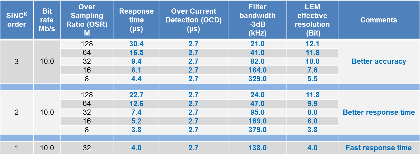
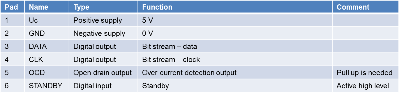
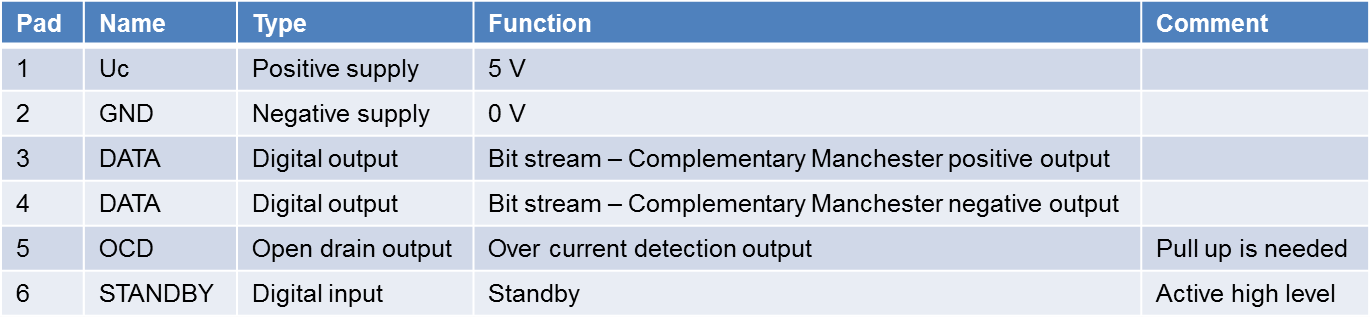
LEM Rogowski Coil (ART)


LEM has developed the ART current Rogowski sensor with the capability to measure up

to 10,000A and beyond. The ART is a raw coil achieving IEC 61869 Class 0.5 accuracy without the need for additional components such as resistors or potentiometers, which have a risk of drift over time.

In addition, the ART labelled “Perfect Loop” has a unique patented coil clasp curing the inaccuracy caused by the sensitivity to the position of the conductor inside the loop. Finally, the ART provides the same ease of installation as split-core current transformers and a better Class 0.5 accuracy. The ART also has the best performance among other Rogowski coil players.


Figure 2: LEM ART features and performances versus competition


What is a Rogowski coil?

A Rogowski Coil is used to make an open-ended and flexible sensor that easily wraps around the conductor to be measured. It consists of a helical coil of wire with the lead from one end returning through the center of the coil to the other end, so that both terminals are at the same end of the coil. The coil length is selected according to the relevant primary cable diameter to provide optimal transfer characteristics.

This technology provides a very precise detection of the rate of change (derivative) of the primary current that induces a proportionate voltage at the terminals of the coil. This is then a current measuring technology only for AC currents. An electronic integrator circuit is usually added to convert that voltage signal into an output signal that is proportional to the primary current. In other words, the Rogowski Coil enables the manufacturing of very accurate and linear current sensors, at the price of additional electronics and calibration.

A  Rogowski coil has a lower inductance than current transformers, and consequently a better frequency response because it uses a non-magnetic core material. It is also highly linear, even with high primary currents, because it has no iron core that may saturate. This kind of sensor is thus particularly well adapted to power measurement systems that can be subjected to high or fast-changing currents. For measuring high currents, it has the additional advantages of small size and easy installation, while traditional current transformers are big and heavy.


Figure 2: Rogowski Coil principle


VOUT = – M*dIP/dt.

M is the mutual inductance between the primary conductor and the coil, which to some extent represents the coupling between the primary and secondary circuits.

The performance of such current sensors highly depends on the manufacturing quality of the Rogowski Coil, since equally spaced windings are required to provide high immunity to electromagnetic interference; the density of the turns must be uniform otherwise the coefficient M could change versus the position of the primary into the aperture.


Another critical characteristic is the closing point that induces a discontinuity in the coil, creating some sensitivity to external conductors as well as to the position of the measured conductor within the loop. The locking or clamping system should ensure a very precise and reproducible position of the coil extremities, as well as a high symmetry while having one of the extremities connected to the output cable. Some new technologies have recently appeared in this area, with special mechanical and electrical characteristics that allows much better accuracy and immunity to the primary cable positioning. While the error due to primary cable position was typically not better than +/-3% in the 50/60Hz frequency domain, it has been reduced to less than +/- 0.5% on some of the latest Rogowski Coil sensors.


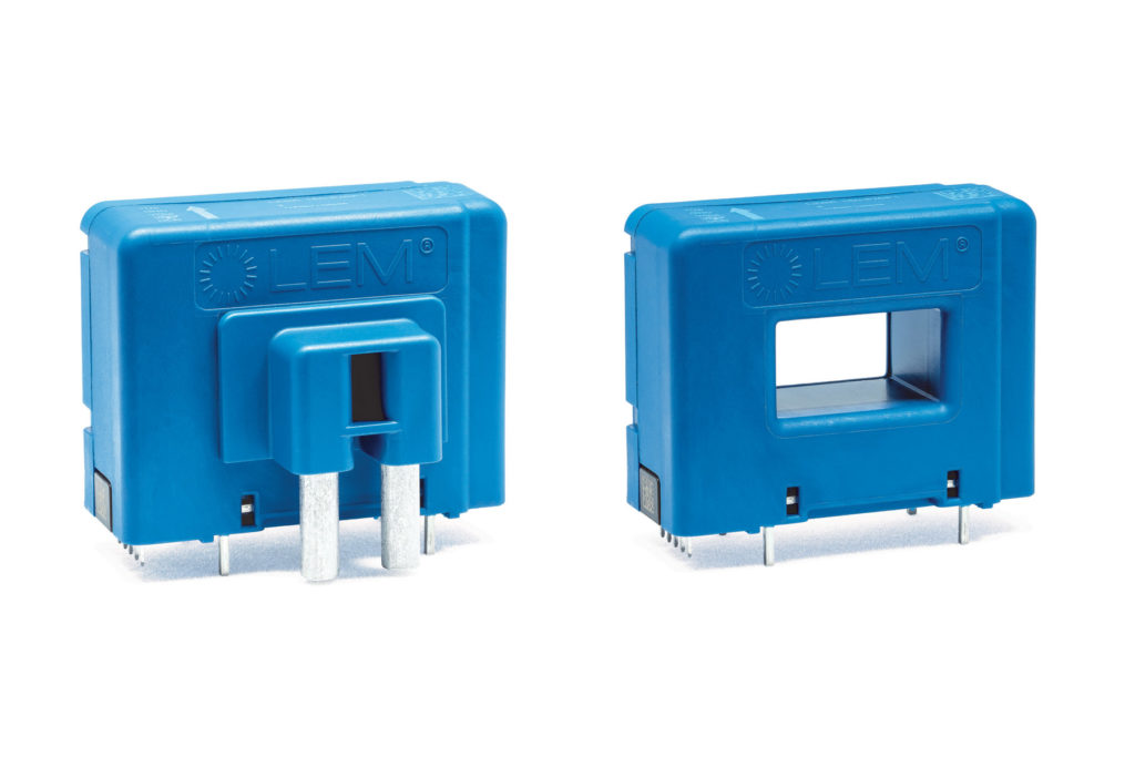
Figure 4: ART Rogowski Coil current sensor from LEM


How LEM managed the challenge:

Two main technics are on the market to make Rogowski coils accurate:

  • The first is to buy standard wound wire on the market and to make the loop connected to a resistor, which will be used for the accuracy calibration.
  • The second is a so-called “pure Rogowski coil” consisting in winding very accurately a regular copper wire all along its length to ensure the final accuracy of the sensor.

While the first is really easy to produce at a low cost, this is nevertheless highly sensitive to external environments, less accurate, and less reliable as it brings in more components.

At the opposite end, the Pure Rogowski coil requires much more investments and knowledge on manufacturing process.

The really thin LEM ART Rogowski coil is part of this second method and has a gain of 22.5 mV/kA; it includes an electrostatic shield to protect against external fields (LEM patent), optimizing performance for small current measurements.

The locking system has also been a key point in achieving the class 0.5 accuracy. And here again LEM had to find an efficient design to make the closure the most efficient possible.

To mask the imperfections on the closing mechanism as well as the connections of the sensor’s secondary wires, LEM engineers created a sleeve acting as a magnetic short-circuit (or more precisely a reluctance short-circuit), virtually bringing together the two sections of the coil located on each side.


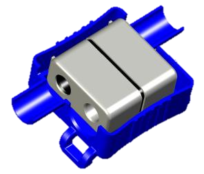
Figure 5: LEM patented Rogowski coil clasp


The sleeve is formed of a piece of ferrite as represented in Figure 5.

This approach was a complete success (LEM patent) – the error associated with the coil clasp has become almost negligible (Figure 6).


Figure 6: Rogowski coil accuracy comparison between a regular Rogowski coil and one using the LEM patented Rogowski coil clasp with primary conductor located at various positions inside the loop.


The accuracy is not only a question of position of the primary conductor in the loop but also of orthogonality, how the primary conductor is crossing the loop, how is it located versus the Rogowski loop axis at 90°, or 45° or 0° or 180° (Figure 7).

Here again, the ART loop is insensitive to this phenomenon and this has no impact on its accuracy thanks to the LEM know-how and patent.


Figure 7: Orthogonality effect. Primary conductor position versus the axis of the Rogowski loop.


Finally, in addition to these high performances, the product had to be easy to use, to install and adapted to any conditions of use.

The ART series provides the same ease of installation as existing split-core transformers, but with the benefits of being thinner (6.1mm diameter) and more flexible.

Whatever the chosen dimension – 35 to 300mm diameter for the coil aperture – the ART can be mounted very quickly by simply clipping it on to the cable to be measured thanks to an innovative, robust and fast twist-and-click closure method. Contact with the cable is not necessary, and the ART ensures a high level of safety as well as providing a high rated insulation voltage (1000V Cat III PD2 – reinforced) and can be used in applications requiring a protection degree up to IP57. Its fixing on the primary cable can be ensured using a cable tie through its expected slot.

The ART also allows disconnection of the coil to be detected through the use of a security seal passed through a specially designed slot, making it really useful when used with a meter (Figure 8).


Figure 8: ART mechanical features: Twist-and-click closure, security seal, and slot to attach the loop to the primary cable.


Intelligent electricity network (smart grid) applications such as power generators, home energy management (HEM), battery monitoring systems (BMS), medium voltage/low voltage substations, sub-metering, electrical vehicle stations, and solar power plants integrate more and more current sensors to ensure reliable integration of distributed renewable energy, energy storage, production and consumption. This leads to the implementation of more current sensors to allow control rooms to automate, monitor remotely and share real-time data of equipment.

With the aim to bring more harmonization in the smart grid landscape, the International Electrotechnical Commission (IEC) builds foundations in every field to provide a strong, resistant and secured electrical grid. Robust and accurate sensors in this network are major challenges to respond to this demanding environment.

IEC 61869 is the new performance standard for sensors, replacing the old IEC 60044 standard for current transformers. ART Rogowski coils sensors are designed and tested against a strict characterization test plan established by LEM experts to comply with and contribute to this evolution. Due to its strong knowledge in accurate measurement, LEM guarantees the measurement repeatability of all of its transducers and accuracy of Class 0.5 according to IEC 61869-2 for ART models for use in future smart cities and their applications.

ART series current sensors are CE marked, UL 2808 recognized and conform to IEC 61869, as well as being covered by LEM’s five-year warranty.

LEM accurate and easy-to-install smart current sensors empower the internet of energy (smart cities).

About LEM

LEM is the market leader in providing innovative and high-quality solutions for measuring electrical parameters for a broad range of applications. LEM answers the demand for an accurate, reliable and easy-to-install energy sensor for future Smart Cities.


Fonte: https://lnkd.in/dwVKAHj

maxresdefault-001

Saiba a diferença entre transdutor por Efeito Hall de Loop Aberto e Loop Fechado

O transdutor é um dispositivo que recebe um determinado sinal de entrada (Pressão, temperatura, potência, intensidade luminosa, vazão, corrente, tensão, etc.), e proporciona um sinal elétrico de saída (tensão ou corrente).

Vale destacar que o transdutor pode ser desde um dispositivo elétrico, eletrônico, térmico, mecânico e até mesmo eletromecânico.

Agora que sabemos sua função, iremos discutir um pouco sobre os transdutores de tensão e corrente.

Estes dois tipos de transdutores são ferramentas essenciais em diversos campos tecnológicos, como industrial, tração (ferroviário e subestações), automação, geração eólica e solar, e também no setor automobilístico.


Transdutores de Tensão e Corrente por Efeito Hall

O conceito mais utilizado nesses dispositivos é o Efeito Hall, descoberto no ano de 1879 pelo físico Edwin Herbert Hall, O efeito Hall é uma propriedade que se manifesta em um semicondutor inserido no “gap” de um campo magnético, gerado pela indução da corrente elétrica a ser medida. Para obter controle do processo, é inserida nesse material uma corrente de controle de tal forma que, quando a corrente elétrica a ser mensurada for zero, a tensão HALL gerada também será zero. Ao circular qualquer corrente diferente de zero, seja ela alternada, contínua, pulsada ou qualquer forma de onda, será gerado no material magnético uma Tensão Hall que será o espelho da onda que induziu esse campo. A amplitude da tensão de Hall varia com a corrente e o campo magnético.

Como o condutor irá produzir um campo magnético que varia com a corrente, é possível utilizar um sensor Hall para medir esta corrente sem interromper o circuito, sendo esta a principal vantagem da utilização deste conceito.

Transdutores por Efeito Hall são classificados em três tipos: transdutor por efeito hall de Loop Aberto (Open Loop – OL) e Loop Fechado (Closed Loop – CL) e o ETA (junção do Loop Aberto com o Fechado).


Transdutor por Efeito Hall de Loop Aberto (Open Loop – OL)

 Os transdutores de loop aberto tem um projeto mais simples do conceito de efeito Hall. Eles geralmente são de tamanhos compactos, mais leves e tem o melhor custo benefício referente à medição do parâmetro de interesse, além de ter um baixíssimo consumo de energia.


Transdutor por Efeito Hall de Loop Fechado (Closed Loop – CL)

Comparado ao transdutor de loop aberto, os transdutores de loop fechado por efeito Hall (também chamados de transdutores por efeito Hall ‘compensados’ ou de ‘fluxo zero’) possuem um circuito compensador que melhora drasticamente o desempenho, ampliando o espectro de frequência e aumentando a precisão.


Transdutores por efeito Hall ETA

A tecnologia ETA em transdutores de corrente por efeito Hall é uma patente da LEM International.

Esta tecnologia se baseia na combinação dos elementos de ambos princípios de loop aberto e loop fechado. O resultado é um dispositivo que tem o melhor balanço entre os benefícios de ambos os princípios de operação. O princípio do loop aberto é fundamentado para a medição da corrente DC e o efeito de transformador (um dos princípios do loop fechado) é usado para medir a corrente AC.

Hoje a LEM possui apenas uma série de transdutor com esta tecnologia, se trata da série LAS.


Agora que você já sabe as vantagens e desvantagens entre eles, escolha a melhor solução!


Fontes: https://www.amds4.com.br/bank/CH24101E.pdf

https://www.amds4.com.br/bank/catalogue_lem_cvt_english.pdf