image

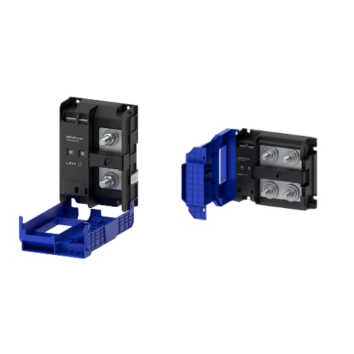
LEM DCES – Medidor de Energia DC

LEM, líder mundial em sensores de corrente e tensão, lançou a nova série DCES, uma linha inovadora de sensores para medição de energia em corrente contínua (DC). Com design compacto, saída digital Modbus RTU e alta precisão, a série DCES é ideal para aplicações modernas que exigem eficiência energética, rastreabilidade e integração com redes industriais.

Principais Vantagens

  • Medição integrada de corrente, tensão, potência e energia
  • Alta precisão: até ±0,2% na tensão e ±0,5% na corrente
  • Interface digital Modbus RTU (RS485)
  • Montagem em trilho DIN
  • Faixa de corrente até 600 A
  • Tensão de operação até 1500 VDC
  • Modelo com ou sem display frontal
  • Operação confiável em -40°C a +85°C

Aplicações Típicas

  • Estações de carregamento de veículos elétricos (EV)
  • Sistemas de armazenamento de energia (ESS)
  • Sistemas fotovoltaicos (PV)
  • Data centers
  • Transporte ferroviário e marítimo com infraestrutura DC
  • Máquinas e equipamentos industriais em DC Bus

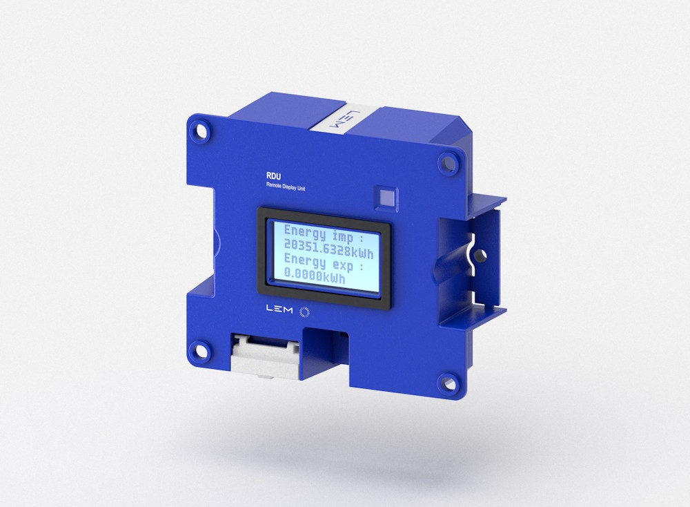
DCES’ remote display unit (RDU)

Resumo Técnico

CaracterísticaValor
Corrente nominalAté 600 A DC
Tensão de entradaAté 1500 VDC
Precisão (corrente)±0,5%
Precisão (tensão)±0,2%
Saída digitalModbus RTU (RS485)
InstalaçãoTrilho DIN
Temperatura de operação-40°C a +85°C
ProteçãoIP20
DisplayOpcional

Fale com a AMDS4

Somos representantes oficiais da LEM no Brasil.

Para mais informações sobre a linha DCES, suporte técnico ou solicitação de proposta, entre em contato conosco:

capa

Nova Série de Transdutores de Corrente FRS e FL – OLCI (Open Loop Coreless Integral)

Sensor de Corrente Integral de Loop Aberto sem Núcleo Magnético

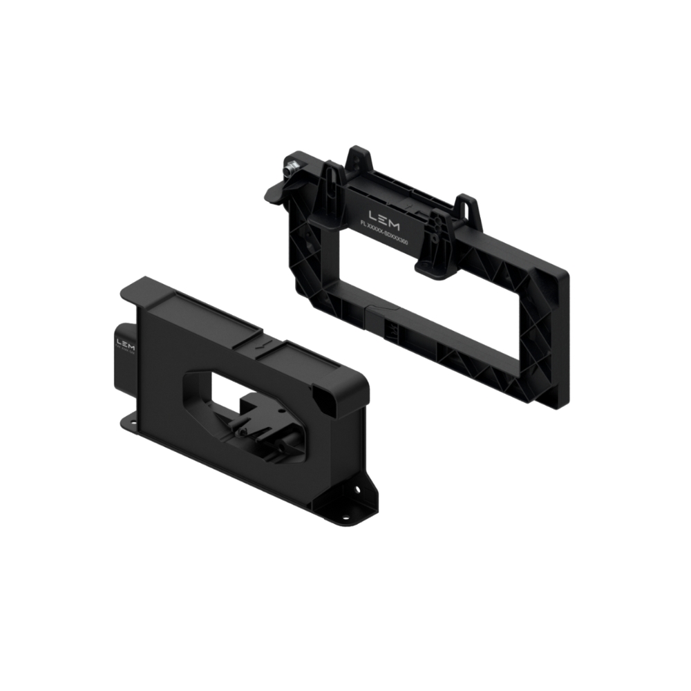
As novas famílias de produtos FRS e FL foram desenvolvidas para a medição eletrônica de correntes contínuas (DC), alternadas (AC) e pulsadas, oferecendo separação galvânica entre os circuitos primário e secundário. Esses sensores inovadores são projetados para aplicações industriais, de tração e ao longo das vias, garantindo medições precisas e confiáveis.

Capacidades e Características dos Sensores FRS e FL

Os sensores FRS permitem a medição de correntes de até 9000 A, enquanto os sensores FL podem medir correntes de até 42 kA. Ambas as famílias de produtos estão disponíveis com saída de corrente (4-20 mA) ou saída de tensão instantânea (0-5 V).

A principal diferença entre as duas famílias está no tamanho do sensor: os sensores FRS possuem uma abertura de 104 mm, enquanto os sensores FL estão disponíveis com aberturas de 200 mm ou 300 mm.

Tecnologia e Vantagens

Utilizando a tecnologia OLCI (Open Loop Coreless Integral), os transdutores FRS e FL garantem medições precisas e confiáveis. Entre as características destacadas dos sensores estão:

– Medição unipolar ou bipolar de correntes primárias até 42 kA.

– Saída de corrente instantânea de 4-20 mA ou saída de tensão instantânea de 0-5 V.

– Alimentação por fonte de +12 ou +24 V DC.

– Separação galvânica entre circuitos primário e secundário.

– Calibração de fábrica.

– Alta largura de banda (> 1 MHz).

– Baixo tempo de atraso (< 400 ns).

Os sensores FRS também apresentam design leve, baixa perda de energia, ausência de offset magnético, baixo consumo e uma ampla gama de dimensões para barramentos retangulares. Além disso, possuem conectores de campo M12.

Aplicações Típicas

Os sensores de alta corrente sem núcleo FRS e FL são amplamente utilizados em diversas áreas industriais devido à sua capacidade de medir correntes DC, AC e pulsadas. Exemplos de aplicações incluem:

– Conversores de energia para turbinas eólicas.

– Eletrolisadores.

– Drives de alta potência.

Conclusão

As famílias de sensores FRS e FL representam um avanço significativo na medição de correntes industriais. Com uma combinação de alta precisão, confiabilidade e flexibilidade, esses sensores são ideais para uma ampla variedade de aplicações exigentes, garantindo desempenho superior e eficiência operacional.

Veja o vídeo oficial de apresentação da fabricante LEM.

Fonte: https://www.lem.com/en/frs-fl

Capa artigo

Bobinas de Rogowski LEM

Conheça as séries da LEM – ART – ARU – AI-PMUL

Série ART & ARU
Bobina de Rogowski split-core (bi-partido), flexível para medição de  corrente CA até 300000 A.
Montagem de clip-on fácil e rápida enquanto o cabo está conectado em qualquer aplicativo de rede de distribuição interna ou externa.
Subestações MV/LV, medição de energia, submedição de edifícios, monitoramento da qualidade da energia.

• Precisão Classe 0.5 sem calibração
• Tensão de isolamento nominal 1kV CATIII
• IP57 (ART), IPx8 (ARU)
• Escudo eletrostático
• Faixa de operação: -40°C a +80°C

Mais informações sobre a série ART: https://www.amds4.com.br/series/14/94/1/ART—RT
Mais informações sobre a série ARU: https://www.amds4.com.br/series/14/106/1/ARU

Série AI-P para bobinas Rogowski.
• Proporciona um erro de linearidade abaixo de 0,1%
• Oferece facilidade de seleção entre 12 faixas atuais, sensibilidades de 6 bobinas De Rogowski e 7 saídas possíveis (TRMS e instantânea, corrente e tensão)
• Montagem em trilho DIN
Mais informações sobre a série AI-P: https://www.amds4.com.br/series/14/103/1/AI-P

img-capa

New LEM’s SMD Current Transducer – HMSR

A Step Forward to Miniaturization for Current Sensing in Power Conversion Systems

Modern power conversion systems must simultaneously become more efficient, smaller and cheaper than previous generation. With this in mind, the Swiss company LEM, global leader in current and voltage sensing, has used its expertise in this field to create a single chip package, the HMSR.

By Damien Leterrier, Thomas Hargé and Stéphane Rollier, LEM


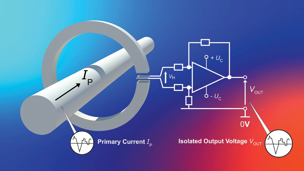
The traditional way to measure current is to use Open Loop Hall effect sensors. The magnetic field created by a current is captured by a magnetic core and measured by a hall element. More recently, dedicated ASICs helped to increase the overall accuracy of the system using advanced compensation techniques.


Figure 1: Open Loop technology principle using a traditional Hall effect chip or a dedicated ASIC


LEM first moved into miniaturization with the LTSR product in the previous decade. At that time, the best way to ensure optimum performances was to use Closed Loop Hall effect technology in combination with a special Closed Loop ASIC designed by LEM. The evolution of ASICs technology enabled the development of Open Loop Hall effect sensors that were capable of approaching the level of performance that Closed Loop technology delivered. Not only did Open Loop technology make it easier to reduce the size of components but it also brought the cost improvements that the market demanded, thanks to it having a simpler structure and lower power consumption. This decade has seen the development of the HLSR series which not only delivers high performance in terms of offset and drift but also excellent response time – and all in a package small enough for PCBAtype applications with only a few mm height.


Figure 2: Evolution of the current sensor’s size over the decades


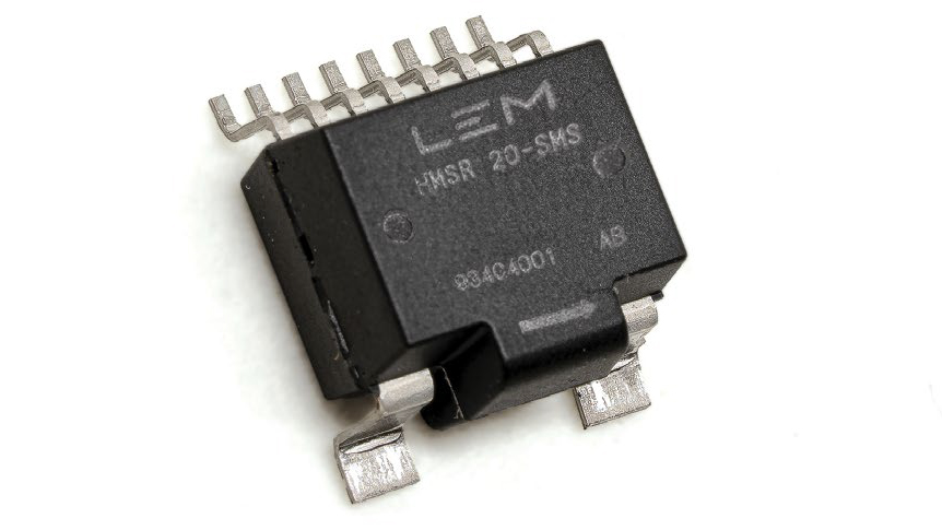
LEM has used the extensive know-how and design expertise that it has accumulated over many years to create the HMSR, a state-ofthe-art current sensor which satisfies the continuous market requirements of cost reduction, performance improvements and miniaturization.


Figure 3: HMSR current sensor


With this new series, LEM is expanding its miniature, current sensors range for AC and DC isolated current measurement. The new HMSR models are easy to use because they include a low-resistance primary conductor (which minimizes power losses), a miniature ferrite and a proprietary ASIC to allow direct current measurement and consistent insulation performance.

This new product category already includes six different nominal currents – 6A, 8A, 10A, 15A, 20A and 30A – with a measurement span of 2.5 times the nominal current available in a SOIC 16 “like” footprint package. Standard models provide an analogue voltage output with different sensitivity levels available, with 5V power supply versions achieving an output voltage of 800 mV @ I PN.

Built-in are two OCD (over current detection) units which separate the control application path to the safety loop. These OCDs are on two dedicated pins – one set internally at 2.93 x I PN as threshold and one externally whose threshold can be adjusted by the user.

However, HMSR sensors should not be seen as simple Open Loop Hall effect ASIC-based transducers. The HMSR unique primary conductor allows overload punctual currents and a high level of insulation. All this is combined with a ferrite-based magnetic circuit to provide excellent immunity against the external inhomogeneous fields found in power electronics applications. This enables the HMSR to be used in environments with high levels of disturbance.

The ferrite used in the HMSR is also a key factor in achieving a high-frequency bandwidth of 270 kHz (-3dB) and makes it possible to achieve good rejection against external fields.

These dedicated ASIC designs combine field-proven techniques such as spinning, programmable internal temperature compensation (EEPROM) for improved gain and offset drifts. The result is high levels of accuracy across a range of temperatures, from -40°C to +125°C with a typical value of 0.5 % of I PN (the HMSR 20-SMS model). Power conversion applications such as solar inverter or drives demand high efficiency levels and these can be reached only if the control loop is accurate.

The accuracy over temperature figures have been greatly improved on the HMSR in comparison to the previous generation of products. The graph below shows the low level of typical overall error across a measured current with the HMSR 20-SMS, as well as very good linearity on a wide temperature range (-40°C to +125°C).


Figure 4: Typical overall accuracy and linearity for HMSR 20-SMS model from -40°C to +125°C)


Figure 5: HMSR response time


However, such accuracy is not enough if it isn’t backed by a fast response time. To this end, the deployment of a fast IGBT, like SiCbased technology, increases the possibility of working with a faster switching frequency – the HMSR is proven to be ready for such demanding technology with a response time below 2uS (see Figure 5).

In multiple applications, HMSR sensors can be mounted directly onto a printed circuit board as SO16 SMD devices, reducing manufacturing costs and providing much needed space-saving for restricted environments. At just 6mm high, the HMSR offers significant space-saving in applications, making it ideal for placing under the heatsink over intelligent power modules (IPMs) (see figure below).


Figure 6: HMSR mounted with IPM


Another area where the HMSR will deliver significant benefits in terms of current measurement is in solar applications.

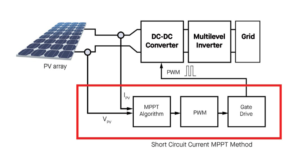
In particular, the maximum power point tracker (MPPT), an important asset in solar energy conversion, is a collection of components that maximize the power generated from a photovoltaic (PV) panel. It does this by regulating current and voltage depending on temperature, sunshine and total resistance of the system. The control system permanently analyses the system output after injecting a small perturbation (using the perturb and observe method). The MPPT then analyses the resulting power (by sensing voltage and current) and deducts the parameter to change in order to reach the MPP (maximum power point). The MPPT then changes the pulse width modulation (PWM) to adapt the voltage of the DC/DC converter.


Figure 7: Maximum Power Point


Figure 8: MPPT architecture


The greater the accuracy and lower the noise, the better the performance from the MPPT will be. Using LEM’s state-of-the art ASIC, the HMSR provides a highly accurate and very low-noise signal which allows the system to operate to its optimal level.

What’s more, string current monitoring makes it possible to compare several strings and to detect issues such as faulty wiring, dirt on the panels and shadows created by growing trees. Here, the excellent accuracy of the HMSR will enable strings to be compared.

In addition, the DC/DC converter used in the MPPT uses highfrequency regulation (around 80kHz), creating high dV/dt which is harmful for electronic components. Thanks to its ruggedized design, the HMSR offers significant resistance to such a noisy environment.

This immunity can easily be checked by applying dV/dt through the sensor and observing the output reaction.

The following graphs (figure 9) show the low disturbance created by applying dV/dt through the sensor. The error generated is only 3% of full scale with a recovery time of 3.8 uS.

HMSR 20-SMS tested with pulsed voltage of +/- 1000 V at 20kV/uS :


Figure 9: Error generated at the HMSR output after applying dV/dt


The two available built-in OCDs on the HMSR will also protect transistors on the inverter from short-circuiting and overload. This kind of detection and protection is an important feature for multiple applications like HVAC on the DC link or motor drive applications. Most modern variable-frequency drives (VFDs) incorporate a motor overload algorithm and the OCD function on the HMSR will make detection much easier, preventing the overheating of equipment. Having two distinct OCDs provides the opportunity to monitor overload and short-circuit events separately.

Of course, isolation requirements could be an issue for the adoption of IC packages when it comes to choosing a current sensor. For example, in the solar industry power plants are often used with higher DC voltages, up to 1500V in order to increase the DC/AC power ratios. This dramatically increases the isolation needed for a current converter.

The long internal distance between primary and secondary sides helps to isolate the primary bar with the rest of the IC, giving a very high level of isolation guaranteed at 4.95kVRMS (at an AC insulation test voltage of 50 Hz, 1 min). This level will be guaranteed for 100% of the shipped products that are tested during production assembly. The special footprint of the HMSR allows 8mm creepage and clearance distances on the landing pad.

A higher comparative tracking index (CTI) means a lower minimum creepage distance is needed and with a CTI of > 600, according to the IEC 62109-1 (Safety of power converters for use in photovoltaic power systems), the working voltage for the HMSR reaches 1600V, which means it is ideally suited to such high-constraint applications.

Another key requirement in the solar industry is that equipment needs to be surge tolerant up to 20kA to offer effective lightning protection. With the HMSR placed directly on to the string inputs that are subject to lightning, components will be extremely robust against such powerful current surges. Indeed, the HMSR has been designed and tested to this level according to the standard 8/20 uS surge test profile.


Figure 10: Typical overcurrent surge profile in solar applications


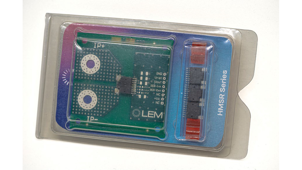
LEM has developed an HMSR evaluation board that makes it possible to prototype and test quickly the extraordinary performances of this new generation of sensors. Available as a sample on request, this new product line will enter mass production in early 2020.


Figure 11: HMSR demo-board available for sampling


IPN 6..30 A
IPM (measuring range) 15..75 A
AC Insulation Test (50 Hz, 1 min) 4.95 kV
Impulse withstand voltage 8 kV
dCp/dCI (mm) 8/8
Operating temperature range -40°C…+125°C
Supply voltage 5V
Step response time 2uS
Frequency bandwidth >270 kHz
Over current detection Yes (x2)
img-cover

New Lem’s Current Sensors – Compact Sizes For Measure Hight Currents

As power electronics systems get smaller, LEM is introducing three new families of compact open-loop current sensors which measure higher currents than earlier sensors of the same size, or similar currents with smaller size. Excellent performance is obtained using a single custom ASIC to perform all signal processing and analog correction functions. This article describes the sensors and their key electrical characteristics. It concludes with some application examples.

Introduction

There are clear trends in current measurement today. For example, in UPS systems, and in power generation from renewable sources, the trend continues towards smaller physical size, higher current ranges, cost savings and quicker response times for faster switching frequencies. The simplicity of open-loop sensors makes them an attractive solution for attaining these objectives.

In this article, we present three new families of sensors that allow the nominal current to be as high as 800 Amps RMS and detection of an overcurrent up to seven times higher. The miniature HLSR xx/SP10 sensors are an extension of the existing HLSR family with an integrated primary conductor. They are mounted on a PCB and are the best choice if small physical size is important. The two other families, HOYS and HOYL (HOYx), are busbar mounted with new magnetic circuits optimized for weight and size. The open-loop HLSR and HO sensors introduced by LEM five years ago, meet the objectives of size, accuracy, speed and cost. However, the nominal primary current of the smaller HLSR is limited to about 50 Amps by saturation of the ferrite magnetic circuit (Reference 1).

Closed-loop sensors have often been used to meet the accuracy and speed requirements of high-current sensors. However, the secondary coil, which cancels the magnetic field from the measured current, adds to the device size, current consumption, complexity and cost. In high-current devices, the secondary must be driven from a high-supply voltage or complex electronics. A preferred approach is to use an open-loop architecture in which the imperfections inherent in an open-loop system are mastered by using a complex ASIC as the magnetically sensitive element. This technique was already used in earlier low-current sensors. Any errors of sensitivity or offset, including drift with temperature, are measured during the ASIC production test and then stored. The corrections needed are applied continuously when it is used, and most electrical parameters approach the level of the previous generation of closed-loop sensors.

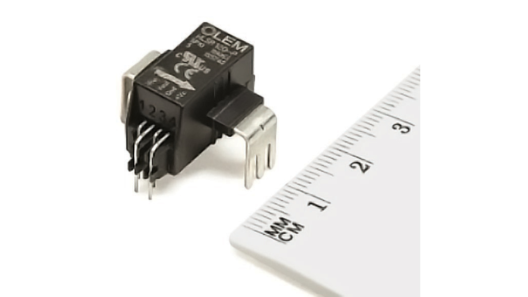
Figure 1 shows one of the high-current HLSR xx/SP10 sensors. It has the same small physical dimensions and footprint as the existing family members, but the maximum nominal current is extended from 50 to 120 Amps by a new FeSi magnetic circuit. In all cases, the maximum current that can be measured is 2.5x the nominal current. The HLSR has an integrated primary and is mounted on a PCB. The four other connections to it are for the secondary side supply, the output voltage (VOUT) and a reference voltage (VREF). VOUT – VREF is proportional to the measured current.


Figure 1: A HLSR xx/SP10 sensor


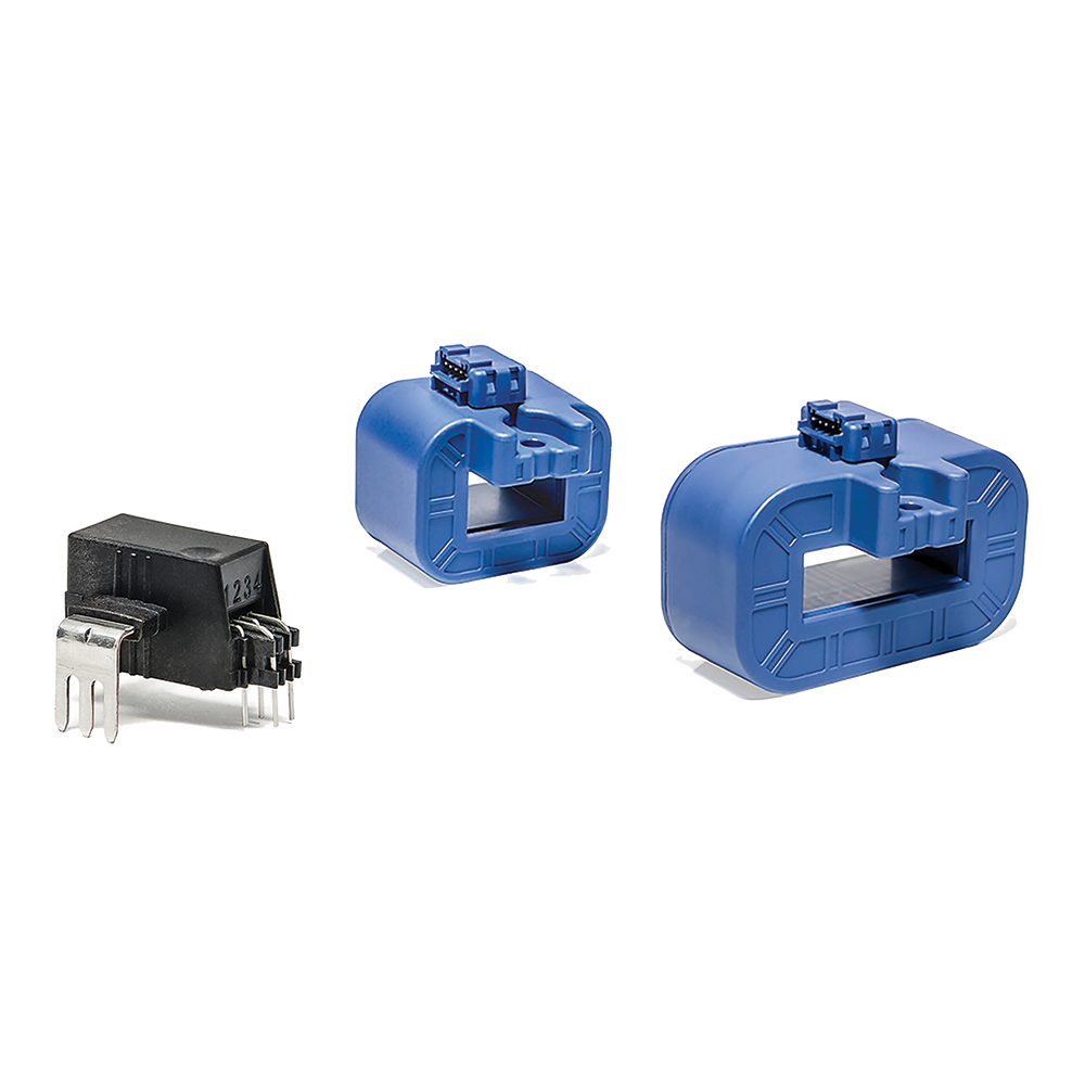
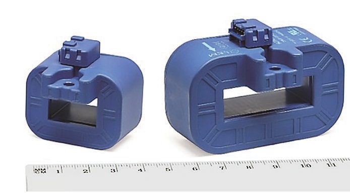
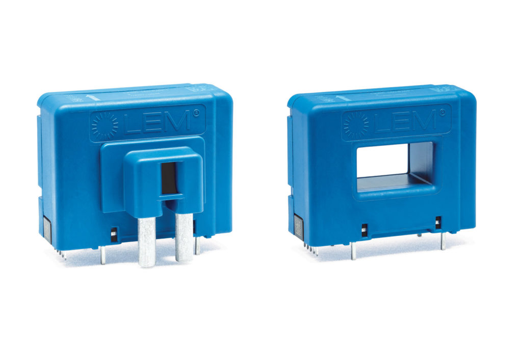
Figure 2 shows the new HOYS and HOYL sensors, which are respectively ‘small’ and ‘large’ devices for mounting on busbars up to 21 x 12 mm and 39 x 12 mm. Together, they cover the current range from 100 to 800 Amps — with a maximum measurable current of 2,000 Amps. These sensors have a fifth output pin, overcurrent detection, which shows that an overcurrent condition has been detected on the primary current. Their compact size is due to the optimization of the magnetic circuit and package around the busbar, and because there are no electronic components inside the sensors except the Hall effect ASIC and two decoupling capacitors.


Figure 2: HOYS (left) sensors & HOYL (right)


Sensor Performance

The supply for the measuring (secondary) side of the sensors is 3.3V or 5V, and the output is referenced to half that value generated by the sensor (although other reference voltage values may be forced from an external source). Apart from the variations in size and mounting arrangement, the differences in performance between the HLSR and HOY families are mainly due to their magnetic circuits.

In sensor applications, switching speeds are rising. Therefore, response times must be shorter so that unusually high current and short-circuit conditions can be quickly detected. In the new sensors, the CMOS ASIC contains Hall cells as the magnetically sensitive element — as well as all signal processing circuits. A high clock speed is used to give a fast response time, less than 3.5 µs, while filters minimize the noise at the sensor output by limiting the ASIC signal path bandwidth to that needed for passing the current waveform.

Two of the most important characteristics of high-current sensors are linearity, and when the primary is part of the sensor, thermal dissipation. A comprehensive series of simulations and tests have been performed to validate these aspects of the new sensors.

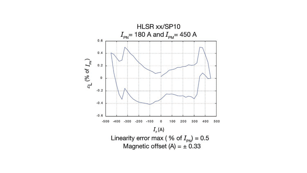
The capability of the HLSR xx/SP10 magnetic circuit was validated by building a test sensor with a I PN of 180 Amps — 50 percent above the highest production value — and measuring its linearity. The result for a current of I PM (+/-450 Amps) is shown in Figure 3a. The curve shows the difference between the measured output and a perfectly linear output. With a maximum of 0.5% of I PN, it demonstrates that the linearity specification for the series sensors is attained with good margin. It’s important to note that short current pulses were used for this test; 450 Amps is too high for a continuous current in the primary.


Figure 3a: Example of linearity & magnetic offset of an HLSR xx/SP10 sensor


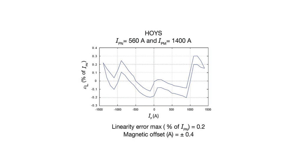
Figure 3b: Example of linearity & magnetic offset of an HOYS sensor


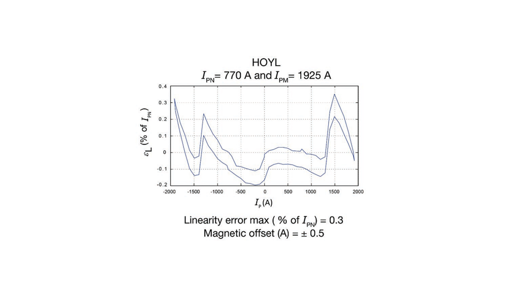
Figure 3c: Example of linearity & magnetic offset of an HOYL sensor


The capabilities of the HOYS and HOYL sensors are shown by their linearity in Figures 3b and 3c respectively. In these tests, the primary current covered the range +/- I PM , but the linearity error is expressed relative to I PN, a more demanding specification.

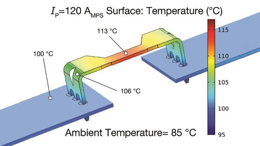
For the HLSR xx/SP10 sensor, whose primary is part of the device, it is important to know the thermal characteristics when a high current passes through it. Clearly, the sensor heating depends upon the PCB to which it is soldered, as well as the sensor itself. Today’s PCB technology allows for maximum currents of approximately 100 Amps. In the simulated example, all four layers of the PCB are used; its design and cooling by natural convection maintain the solder joints at 100 ºC in a 85 ºC environment. Figure 4 shows the results – only the sensor primary is shown. However, the simulation is situated as usual in the sensor housing. With a current of 120 Amps DC, the hottest part of the primary stabilizes at 113 ºC, just lower than the 120 ºC maximum allowed.


Figure 4: Thermal simulation of the primary of an HLSR xx/SP10 sensor


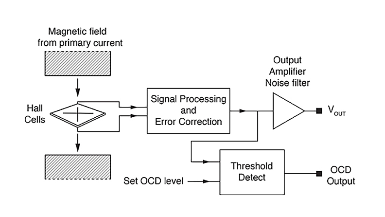
A particularly useful feature of the HOYx sensor family is overcurrent detection (OCD). The input used for OCD is taken before the sensor output amplifier and filters – see the simplified block diagram of Figure 5. This has two advantages: 1) the signal here is of lower amplitude, so a current level higher than that which saturates the sensor output can be detected; and 2) the OCD response time is faster than that at the output.

By default, the OCD threshold is set at 2.93x I PN, but 15 other multiples from 0.68x I PN to 7.06x I PN may be selected at the time of ordering the sensor. The exact multiples available are shown in the datasheets (Reference 2): In the most extreme case, an OCD level of 5,648 Amps may be chosen for the 800-Amp version of the HOYL sensor. Note that OCD levels are only accurate up to 10% or 20%, depending upon the level chosen. This is more than sufficient for the fast warning function that the OCD performs.


Figure 5: The OCD system


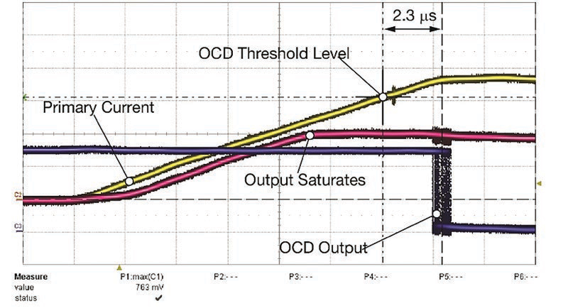
Figure 6 shows an example of the OCD output. The primary current (yellow) is ramped up above the level saturating the sensor output (red); 2.3 µs after the OCD threshold is crossed, its output (blue) falls to 0V. The OCD output is an open drain, which allows several to be connected to a single warning line. The spread of OCD response times is due to the primary current not being synchronized with the sensor clock.


Figure 6: Current and sensor waveforms when the OCD is triggered


The new sensors have excellent isolation characteristics. In all of the HLSR and HOY sensors, there is full galvanic separation between the primary and secondary circuits. For example, the 1.2/50 µs ‘impulse withstand’ insulation test allows 8 kV with the HLSR sensors and 9.6 kV with the larger HOYL family.

Sensor reliability is another important consideration. The construction of open-loop current sensors is extremely simple, with only one active component – the Hall effect ASIC – and very few solder joints (none at all in the case of the HLSR family). The reliability of this sensor type is therefore excellent, with a FIT rate of 3.4 — corresponding to a MTTF of 294,170,980 hours.

Table 1 shows a summary of the principal electrical characteristics of the HLSR xx/SP10 and HOYx sensors. Complete details can be found in the product datasheets.


Table 1

Parameter HLSR xx/ SP10 HOYS / HOYL Comment
Nominal Current,

IPN (A)

80 – 120 100 – 800  
Maximum Current, IPM (A) 200 – 300 250

2000

 
VOUT – VREF (mV) 800 800 5V supply; Input current = IPN
Response time (µs) 2.5 3.5  
Bandwidth (-3dB) (kHz) 250 180 / 140 Small signal
Noise at the output (mVpp) 8.8 5.8 8.6 In 100 kHz bandwidth
OCD available No Yes  
Overall accuracy ( of IPN) +/-1.0 +/-1.0 to

+/-1.25

At 25 ºC
Overall accuracy ( of IPN) +/-3.8 +/-3.8 to

+/-4.0

At 105 ºC
Impulse withstand voltage (kV) 8 9.6 1.2/50 µs rise/fall
Footprint (CM2) 3.87 11.0 /

17.8


Application Example 1: UPS Get Smaller

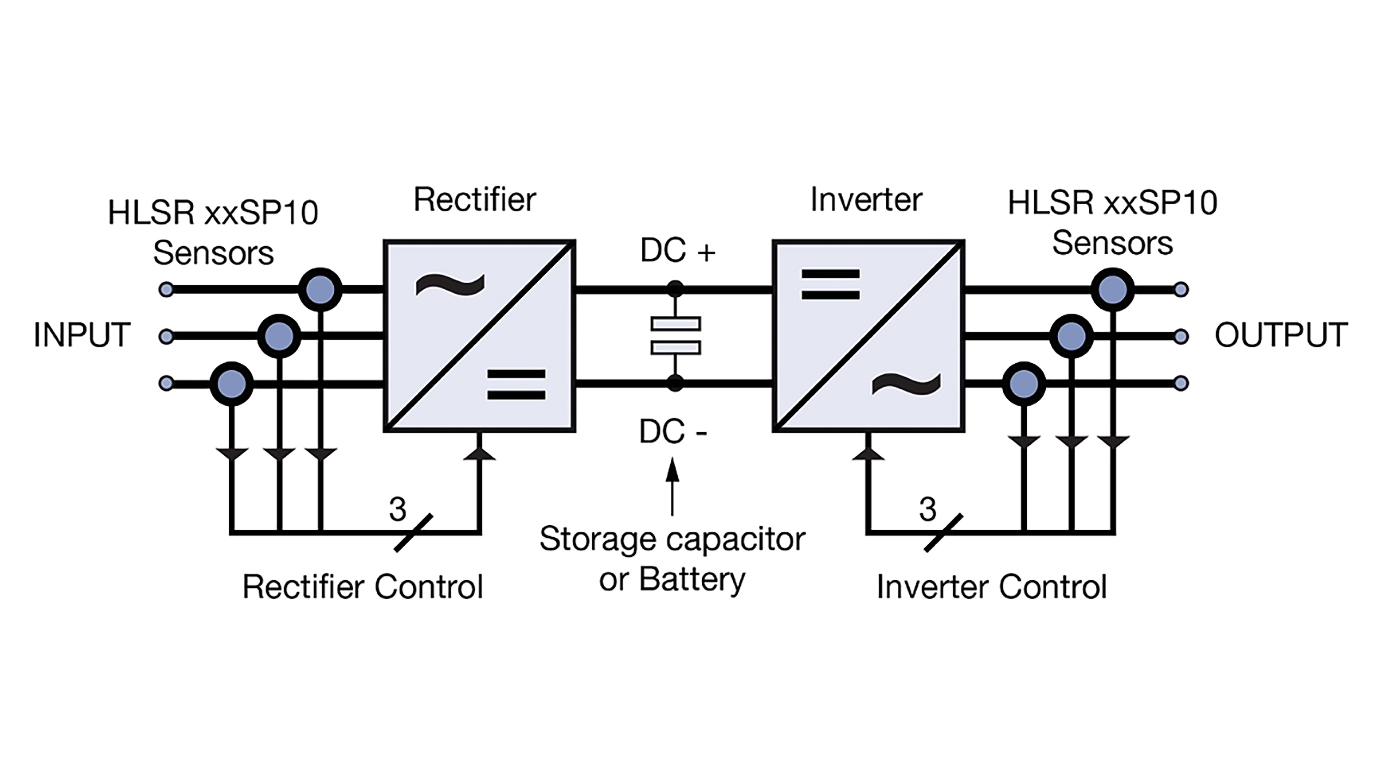
Uninterruptible Power Supplies (UPS) are being driven by two technology trends. Faster switching devices allow lower value reactive elements to be used; these are physically smaller so the electronics can all be PCB mounted. Current sensors also have to follow the same size trend, so as to avoid dominating the PCB surface. At the same time, higher currents can be passed by using many or all of the layers on multi-layer PCBs – some layers may be thick and dedicated to high current capacity. The HLSR xx/SP10 sensor is ideally situated at the intersection of small size, high current ranges and PCB mounting. Figure 7 shows a simplified application schematic in which HLSR xx/SP10 may be used in the control loop for the switches used both for AC to DC and DC to AC conversion.


Figure 7: HLSR xx/SP10 sensors in a UPS system


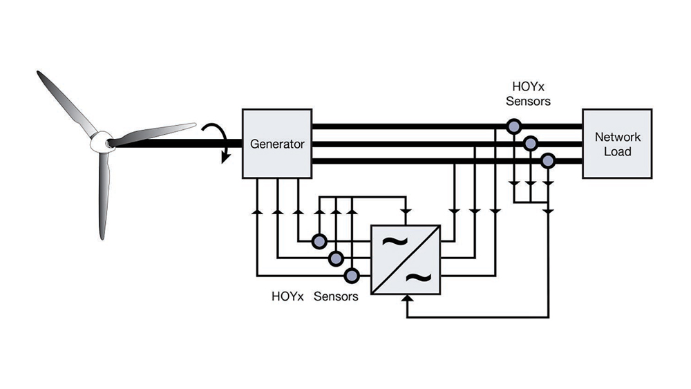
Figure 8: HOYx sensors in a wind turbine system with LVRT


Application Example: Large Measuring Range and OCD For Wind Turbines

In this application, the large current measuring range and the OCD feature of the HOYx sensors can be useful. The generator driven by a wind turbine may use power from the network it drives for its stator coils. See Figure 8. When mixed with AC current from the generator, the AC/ DC converter output creates the correct 50 Hz waveform for the powered network. If the network load draws too much current, power available for the generator may become insufficient, worsening the effect of the excessive load and, if there is no Low Voltage Ride-Through (LVRT) capability, the failure of one generator may propagate through the network and cause others to fail. Part of the LVRT solution is to detect overcurrent on the network side, where the large measuring range of the HOYx sensors is advantageous; the OCD feature is useful to decide different corrective actions and to confirm that current spikes have disappeared. The small physical size of the HOYx sensors makes them easy to deploy in these applications.

Conclusion

This article has introduced new sensors allowing currents of up to 2,000 Amps, to be measured using simple, low cost, open-loop architecture. In many cases, their performance will allow them to be used in place of more complex sensors. The compact size, low-supply voltage and OCD feature of the HOYx sensors will give designers new possibilities to implement efficient and economic systems.

Reference (1): https://www.lem.com/en/file/3135/download

Reference (2): https://www.lem.com/en/product-list?keys=HOYL
and https://www.lem.com/en/product-list?keys=HOYS

artigo

Comparação Shunts, Transformadores e Transdutores

INTRODUÇÃO

Uma aplicação muito frequente na indústria de sensores magneto-resistivos é o sensoriamento da intensidade da corrente que circula num circuito. Esse sensoriamento serve para realimentar os circuitos de controle PWM que determinam a velocidade e potência de motores, acionamento de solenoides, e muitos outros dispositivos semelhantes. Uma das aplicações mais comuns é a realimentação dos circuitos de controle de motores.


Para se obter um sinal proporcional à corrente que circula por um condutor, existem diversas tecnologias que são utilizadas nos componentes comerciais.

Essas tecnologias incluem shunts resistivos, transdutores de efeito hall, transformadores de corrente e bobinas de Rogowski.

Cada tecnologia tem suas vantagens e desvantagens como, por exemplo, a não existência de isolamento no caso do shunt ou ainda a queda de tensão no circuito causando perdas, etc.

Os sensores magneto-resistivos oferecem muitas vantagens que, quando analisadas, podem torná-los uma escolha melhor do que as outras opções.  Dentre as vantagens que destacamos para esses sensores, está o fato de que proporcionam isolamento elétrico total, não causam alterações na intensidade da corrente do circuito sensoriado e, além disso, são rápidos o bastante para poderem operar com frequências tão altas como 5 MHz, numa faixa dinâmica de 100 dB.


TIPOS DE SENSORES DE CORRENTE

Shunts Resistivos

Resistência de derivação para medição de corrente contínua. O Shunt é principalmente empregado para medições de correntes elevadas, sendo calculado de tal maneira que, a uma determinada corrente nominal, se tenha uma queda de tensão, geralmente de 60, 150 ou 300 mV.

Para obter uma indicação de corrente, deve ser conectado ao shunt um indicador bobina móvel com escala igual à corrente nominal e o campo equivalente à queda de tensão provocada pelo shunt.

Para que seja assegurada a precisão do shunt, deve-se tomar o cuidado para que não sejam conectadas linhas de medição com resistência maior que o valor mencionado nos dados técnicos do shunt.


Exemplo de Dados Técnicos do shunt

Norma: NBR 5180
Terminais: Latão MS 58.
Conexão: Ao barramento através de parafusos de aço niquelado ou latão à linha de medição através de parafusos de latão com cabeça cilíndrica, M5x8.
Material da Resistência: Manganín.
Resistência da Linha de medição:
Shunt 60 mV ≤ 0,35 Ω
Shunt 150 mV ≤ 4 Ω
Shunt 300 mV ≤ 12 Ω
Classe de exatidão: 0,5%.
Sobrecarga de curta duração:
In até 500A 10 x In/5 seg.
In de 501A/2000A 5 x In/5  seg.
In de 2001A/10000A 2 x In/5 seg.

Transdutores de Efeito Hall

São dispositivos que utilizam o princípio de efeito Hall para a medição de corrente, com a capacidade de medir sinais AC e DC, com total isolamento galvânico entre o circuito primário (alta potência) e secundário (circuito eletrônico).  Podem trabalhar com vários formatos de onda (faixa ampla de frequência).


Os sensores de corrente por efeito Hall de malha fechada podem medir correntes AC e DC numa faixa ampla de frequência. Dessa forma, possuem a capacidade de reproduzir praticamente qualquer formato de onda. Possuem uma saída em corrente determinada através de uma relação entrada / saída. Em modelos, por exemplo, que possuem uma relação de 1:1000,  teremos na saída do sensor um sinal que é espelho do primário, numa proporção 1000 vezes menor.
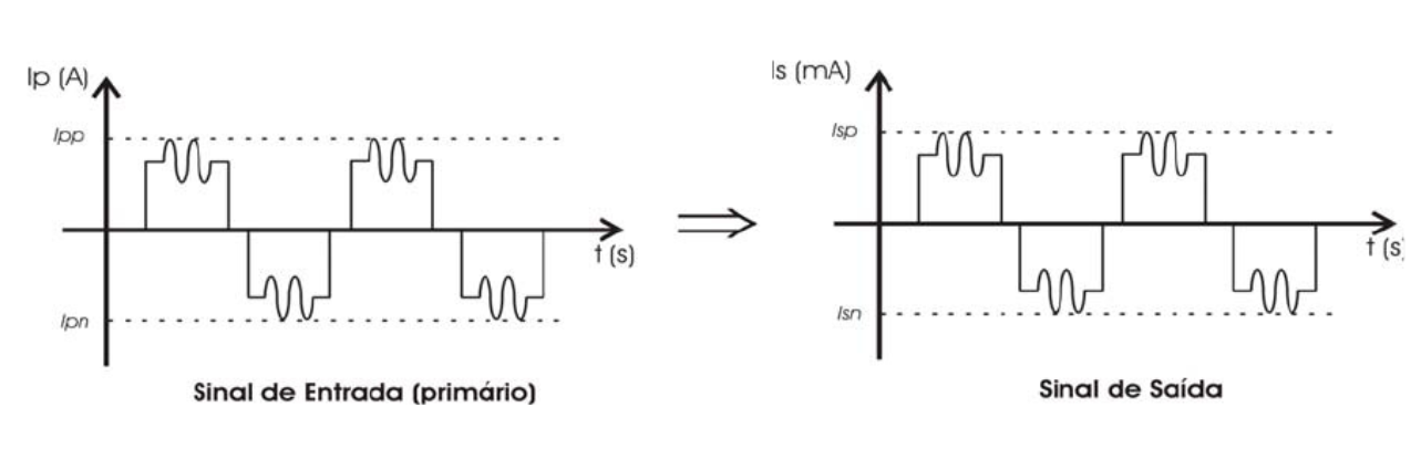


Na escolha do modelo a ser utilizado, deve-se observar quais são os valores de corrente de pico positivo (Ipp) e negativo (Ipn), pois os mesmos devem respeitar a faixa de medida do sensor selecionado.

Por exemplo:

Pegando-se um modelo cuja faixa de medida seja ± 80 Adc, o Ipp e o Ipn, devem ser, respectivamente, +80Adc e -80Adc.

A corrente nominal tem um papel importante na indicação do erro do sensor. Como os mesmos podem medir vários formatos de onda, basear-se somente neste parâmetro para dimensionar o sensor pode acarretar em erro, pois os valores Ipp e Ipn podem extrapolar os valores da faixa de medição.

A conversão do sinal de saída em corrente para tensão é feita através de resistores implementados na eletrônica interna do próprio transdutor, ou na montagem da placa, onde é instalado em série entre a saída e o terra (GND).
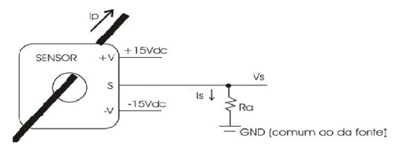


Em medições de corrente com baixa amplitude do sinal, pode-se aumentar a resolução da medida, fazendo com que o condutor seja passado mais de uma vez pela janela do sensor.
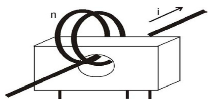


A corrente lida pelo sensor será o resultado do número (n) de vezes que o condutor será passado pela janela do sensor, multiplicado pelo valor da corrente (i) que passa pelo condutor. Exemplo:

número de vezes que o condutor passa pela janela: n = 5
corrente no condutor: i = 5A

Valor da corrente que o sensor fará a leitura: n x i = 5× 5 = 25


Algumas vantagens e aplicações destes sensores:

– Medição de corrente contínua: Substituição com vantagem de custo-benefício os sensores semicondutores de efeito Hall e seu complexo sistema eletrônico de calibração e compensação de temperatura.
– Proteção de sistemas de energia em corrente contínua: substitui o shunt resistivo de potência, eliminando problemas de dissipação de calor.
-Banco de baterias para alimentação de sistemas de proteção em subestações: diferentemente dos shunts, é dispensável o uso de amplificadores de alto ganho, que são susceptíveis às interferências eletromagnéticas externas.
-No-breaks: por não usar shunt, os transdutores de efeito hall dispõem de uma perfeita isolação galvânica entre circuito primário e secundário.
-Carregadores de baterias automotivas e tracionarias: excelente sensibilidade para uma vasta gama de correntes.
-Medição e controle de processos em indústria eletroquímica:

Maior robustez, sendo indicado para ambientes agressivos. Pode suportar atmosferas com poeira e outros poluentes, calor, umidade, elevada interferência eletromagnética e vibração, sem alterar o seu funcionamento normal, nem sua precisão (verifique as características técnicas de cada modelo).

-Controle de processo em galvanização: menor custo.
– Otimização de layout, por se tratar de uma tecnologia mais avançada, que além de substituir os shunts e transformadores em um único componente [pois mede AC (Transformadores) e DC (Shunts)], seu tamanho é reduzido em comparação às outras opções.

Sua principal desvantagem é que na maioria das vezes seu custo é mais elevado que os transformadores e shunts, porém, se forem consideradas todas as vantagens, os transdutores são as melhores opções para desenvolver um projeto confiável e de qualidade.


Tipos de transdutores:

Transdutores de corrente com janela possuem um sistema de medida direta que dispensa a utilização de TCs ou SHUNTs. Basta a passagem do condutor pelo próprio transdutor, obtendo a medida AC ou DC com total isolamento galvânico.

Transdutores de corrente com terminais: geralmente utilizados em medidas de baixo valor de corrente. Nestes modelos, o condutor deve ser fixado nos terminais do transdutor.


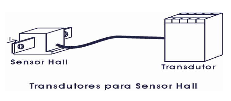
Transdutores de corrente que utilizam sensor hall externo: Utilizados para medidas AC e DC. Diferentemente dos modelos com janela e de terminais, que possuem os pontos de medida da corrente integrados no próprio corpo do transdutor, o modelo com sensor externo possui padrão DIN de fixação em fundo de painel, necessitando dos sensores (sondas) de corrente AC e DC (Efeito hall realimentado) para executarem as medidas. Eles são ideais em casos onde a amplitude da corrente ou os pontos de medida estão localizados remotamente (ao longo do painel).


Transdutores de corrente que utilizam TC (Transformador de Corrente): Utilizados para medidas AC. Os mesmos são ideais em casos onde a amplitude da corrente ou os pontos de medida estão localizados remotamente (longe do painel).


Multiplexador (Concentrador): Em casos onde existem vários pontos de medida que precisam que os seus dados sejam enviados para um único local (equipamento), pode-se utilizar o Multiplexador (Concentrador) que recebe as informações de vários transdutores e as concentram em uma única saída.


Transformador de Corrente

Os transformadores de corrente são classificados em dois tipos:

-Transformadores de corrente para serviços de medição, utilizados para medição de correntes em alta tensão, possuem características de boa precisão (ex.: 0,3%-0,6% de erro de medição) e baixa corrente de saturação (em torno de 4 vezes a corrente nominal).
-Transformadores de corrente para serviços de proteção, utilizados para proteção de circuitos de alta tensão, são caracterizados pela baixa precisão (ex.: 10% -20% de erro de medição) e elevada corrente de saturação (na ordem de 20 vezes a corrente nominal).


Quando a corrente em um circuito é muito alta para ser aplicada diretamente em algum instrumento de medição, um transformador de corrente produz uma corrente reduzida exatamente proporcional à corrente no circuito, que pode ser facilmente conectado ao equipamento de registro. Um transformador de corrente também isola os instrumentos de medição do que pode ser muito alta tensão no circuito monitorado. Transformadores de corrente são comumente usados em medição e relés de proteção na indústria de energia elétrica.

Um transformador de corrente ou simplesmente TC é um dispositivo que reproduz no seu circuito secundário, a corrente que circula em um enrolamento primário com sua posição vetorial substancialmente mantida, em uma proporção definida, conhecida e adequada. Os  transformadores  de corrente, também chamados de transformadores de instrumentos, utilizados em aplicações de alta tensão (situações essas onde circulam, frequentemente, altas  correntes),  fornecem correntes suficientemente reduzidas e isoladas do circuito primário de forma a possibilitar o seu uso por equipamentos de medição,  controle e proteção. Como qualquer outro transformador, um transformador de corrente tem um enrolamento primário, um núcleo magnético e um enrolamento secundário.  A corrente alternada que flui no primário produz um campo magnético no núcleo, que então induz uma corrente no enrolamento do circuito secundário.        O principal objetivo do projeto transformador de corrente é o de assegurar que os circuitos primário e secundário estejam acoplados de forma eficiente, de modo que a corrente secundária tem uma relação exata para a corrente primária.
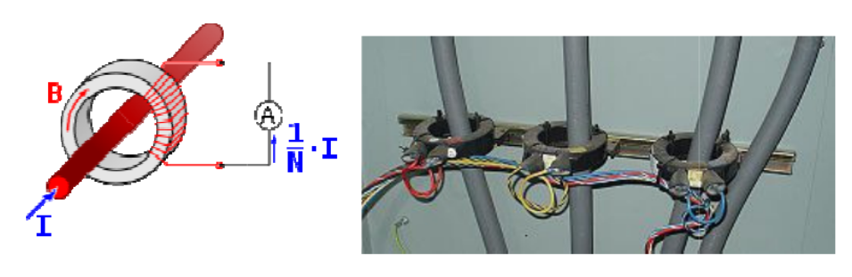


Os designs mais comuns de TC são constituídos por um comprimento de fio enrolado muitas vezes em torno de um anel de aço-silício passando no circuito a ser medido. O circuito primário do TC, portanto, consiste em um único ‘virar’ do maestro, com um derivado de muitas centenas de voltas. O enrolamento primário pode ser uma parte permanente do transformador de corrente através do núcleo magnético. Os modelos com janela também são comuns, que podem ter os cabos do circuito inseridos no meio de uma abertura no centro, para fornecer um único turno no enrolamento primário. Quando os condutores não são centrados na janela do transformador, pequenas imprecisões podem ocorrer.

Formas e tamanhos podem varias de acordo com o usuário final ou fabricante do quadro. Exemplos típicos de baixa tensão razão simples de medição de transformadores de corrente são o tipo de toque ou caso plástico moldado.

Transformadores de corrente de alta tensão são montados em buchas de porcelana para isolá-los da terra. Algumas configurações do TC têm deslizamento em torno da bucha de um transformador de alta tensão ou disjuntor, que mantém automaticamente os centros de condutores dentro da janela do TC.


Tipos Construtivos

São classificados de acordo com o modelo de enrolamento primário, já que o enrolamento secundário é constituído por uma bobina com derivações (taps) ou múltiplas bobinas ligadas em série e/ou paralelo, para se obter diferentes relações de transformação.  Quanto aos tipos construtivos, os TCs mais comuns, são:


-Tipo enrolado: Este tipo é usado quando são requeridas relações de transformações inferiores a 200/5. Possui isolação limitada e, portanto, se aplica em circuitos até 15 kV. Ocorre quando o enrolamento primário é constituído de uma ou mais espiras que envolvem o núcleo do transformador.
– Tipo barra: Transformador de corrente cujo enrolamento primário é constituído por uma barra, montada permanentemente através do núcleo do transformador.
– Tipo bucha: Consiste de um núcleo em forma de anel (núcleo toroidal), com enrolamentos secundários. O núcleo fica situado ao redor de uma “bucha” de isolamento, através da qual passa um condutor, que substituirá o enrolamento primário. Este tipo de TC é comumente encontrado no interior das “buchas” de disjuntores, transformadores, restarters, etc..
– Tipo janela: Tem construção similar ao tipo bucha, sendo que o meio isolante entre o primário e o secundário é o ar. O enrolamento primário é o próprio condutor do circuito, que passa por dentro da janela.
– Tipo Núcleo Dividido: Transformador de corrente tipo janela em que parte do núcleo é separável ou basculante, para facilitar a passagem do condutor primário.
– Tipo com vários enrolamentos primários: Transformador de corrente com vários enrolamentos primários distintos e isolados separadamente.
– Tipo com vários núcleos: Transformador de corrente com vários enrolamentos secundários isolados separadamente e montados cada um em seu próprio núcleo, formando um conjunto com um único enrolamento primário, cujas espiras enlaçam todos os secundários.

Bobina de Rogowski

Nomeada em homenagem ao físico alemão Walter Rogowski, a Bobina de Rogowski é um dispositivo elétrico usado para medir corrente alternada (AC), exemplos: transiente de alta velocidade; correntes pulsadas ou correntes senoidais de alta frequência.

Na sua forma mais simples, uma bobina de Rogowski é uma bobina enrolada uniformemente de N voltas por metro em um núcleo não magnético de área transversal constante. O fio de enrolamento retorna ao ponto de partida ao longo do eixo central da primeira passagem, e as duas extremidades são tipicamente conectadas a um cabo. A extremidade livre da bobina é normalmente inserida em um soquete adjacente à conexão do cabo de uma maneira que permite que ele seja desconectado, permitindo assim que a bobina seja enrolada em torno do condutor que transporta a corrente a ser medida.

Uma das vantagens de uma bobina de Rogowski sobre outros tipos de transformadores de corrente é que ela pode ser feita aberta e flexível, permitindo que seja envolvida em torno de um condutor vivo sem perturbá-la. 

Uma vez que uma bobina de Rogowski tem um núcleo de ar, ao invés de ferro, faz com que ela possua uma baixa indutância e pode responder a rápidas mudanças de correntes. Também, porque não tem nenhum núcleo de ferro para saturar, é altamente linear, mesmo quando submetida a grandes correntes, como os usados em transmissão de energia elétrica (podendo substituir um enorme transformador por uma pequena e leve bobina), solda, ou aplicações de pulso. Uma bobina de Rogowski projetada corretamente, com enrolamentos igualmente espaçados, é praticamente imune às interferências eletromagnéticas.

Recentemente, sensores de baixo custo com base no princípio de Rogowski  têm  sido  desenvolvidos.  Estes sensores compartilham os princípios de uma bobina de Rogowski, sendo que a medição da taxa de variação da corrente utiliza um transformador sem núcleo magnético.   A diferença entre a bobina de Rogowski tradicional é que o sensor pode ser fabricado usando uma bobina planar ao invés de uma bobina toroidal. Para rejeitar a influência de condutores de fora da região de medição dos sensores, estes sensores planares de Rogowski utilizam uma geometria da bobina concêntrica em vez de uma geometria toroidal, limitando a resposta aos campos externos.  A principal vantagem desse sensor planar é que o enrolamento de precisão, que é uma exigência, pode ser obtido utilizando uma placa de circuito impresso de baixo custo de fabricação.


Tabela Comparativa

Sensor de Corrente Tipo de Medição Precisão Tamanho Segurança Custo
Transdutor de Corrente AC+DC Alta Compacto Alta Baixo/Alto
Transformador de Corrente AC Baixa Médio/Grande Média Baixo/Alto
Shunt DC Baixa Compacto/Médio Média Baixo
Bobina de Rogowski AC Alta Compacto Alta Baixo/Alto


Informações da tabela representa uma média geral.

Para ter informações mais precisas, verifique os modelos e necessidades para cada aplicação.

Entre em contato através do e-mail amds4@amds4.com.br, para eventuais dúvidas e necessidades.
SIGMA_Poster_2019

Nova Série de Transdutores de efeito Hall com desempenho Fluxgate

Série LES-LESR-LKSR-LPSR-LXS-LXSR


A nova série possui tecnologia de efeito hall de loop fechado, porém, devido aos estudos realizados pelo setor de desenvolvimento da LEM, estes novos transdutores alcançaram a performance de precisão e medição da tecnologia Fluxgate, assim destacando-se de seus concorrentes e as séries de tecnologia semelhante da própria LEM.

Características:

– Feito sob a patente ASIC LEM de efeito Hall para alto desempenho em loop fechado.

– Diversas opções de correntes nominais, de 1,5 a 50 A nominal.

-Compatíveis com as séries anteriores: LTS, LTSR, CAS, CASR e CKSR.

– 22 modelos com várias opções de: referência, base, janela ou PCB, detecção de sobre corrente (modelo LPSR).

– Drift do offset  reduzido em 4 ppm/K.

Quadro de Comparação:


Série CAS-CASR- CKSR: https://www.amds4.com.br/series/1/65/1/CAS—CASR—CKSR

Série LTS-LTSR: https://www.amds4.com.br/series/1/26/1/LTS—LTSR—LTSP

Série LES-LESR-LKSR-LPSR-LXS-LXSR: https://www.amds4.com.br/series/1/53/1/LES—LESR—LKSR—LPSR—LXS—LXSR

img-08

FLUXGATE TECHNOLOGY AND THE NEW HIGH ACCURACY CURRENT TRANSDUCER (IN 2000)


Technology innovations take fluxgate current transducers to previously unattainable performance levels.


The use of fluxgate technology in transducers for precise current measurement is well-known. In order to improve performance beyond that of existing sensors new ideas are needed. This article starts with a short overview of fluxgate-based current transducers, and then it shows how applying innovations to this architecture has allowed the development of a new family of transducers. Several related improvements must be made together, and the result is a compact transducer which maintains its accuracy over a wider temperature range and has a reduced noise level. The improved performance parameters and some key results of the product characterization will be presented.


Introduction to fluxgate current transducers.


The fluxgate current transducers described in this article are closed loop devices in which the magnetic field created in a magnetic circuit by the measured or primary current, IP, is exactly cancelled by a secondary or compensation current, Icomp, passed in a coil of Ncomp turns around the same magnetic circuit. In the general case where the primary current may have Np turns, IP is simply given by:


IP = Icomp x Ncomp / Np


The zero-field condition is detected by a fluxgate, which consists of a coil wound around a ferromagnetic core that saturates in the presence of a magnetic field. The inductance of the coil reduces when the core saturates. If a symmetrical square-wave voltage drives the fluxgate the rate of change of its current will increase when it saturates but the current waveform will be symmetrical unless a magnetic field due to the primary current is additionally applied, in which case the waveform will be asymmetric.


Figure 1. (a) Fluxgate drive waveform; (b,c) Fluxgate current in the absence and presence of an external magnetic field.


This is shown in figure 1: trace (a) shows a square applied voltage waveform, which has only odd harmonics of the fundamental frequency; trace (b) is the symmetrical current waveform obtained when the external magnetic field is zero; it also has only odd harmonics; trace (c) shows an asymmetric waveform when the external field is not zero; this waveform contains even harmonics and a DC component.


Figure 2 shows the operating principle of a current transducer using this principle. The square wave voltage is applied to the fluxgate with the H-Bridge; its current is converted to a voltage by resistance R, and its symmetry is measured by a signal treatment such as detecting the second harmonic of this waveform. The loop is completed by driving the compensation current with the Class AB amplifier such that this second harmonic is zero. Icomp is converted to a voltage by Rm.


Figure 2. Operating principle of a fluxgate transducer.


Note that the fluxgate system covers the DC and low frequency range of the primary current; for higher frequencies the current transformer effect is used directly, as well as other techniques described later.


Advantages and limitations of fluxgate current transducers.


The fluxgate is a passive element which is driven symmetrically; together with the use of the second harmonic to detect zero field this gives a system whose offset – and, more important, whose offset drift – is low, being principally constrained by the electronics of the feedback system. The turns ratio Ncomp / Np is exactly known, so the transducer is very accurate and stable. It operates at zero magnetic field provided that the loop gain is high enough, which gives a system having excellent linearity. The transformer effect allows for a good response at high frequencies. Unlike a Hall-cell based transducer there is no sensing element with a high resistance so the white noise is low.


However there are some limitations.


The voltage drive which excites the fluxgate may couple into the secondary current and add an unwanted signal, or ripple, at the excitation frequency. This can be overcome by driving a dummy fluxgate in anti-phase to the one used in the measurement loop, though the effectiveness of this is limited by the fluxgate matching.


In general the fluxgate loop will not function up to the frequency at which the transformer effect takes over. This frequency gap must be filled – for example, by a pick-up coil whose output voltage is proportional to the rate of change of the primary current; after integration this signal is summed with the output of the second harmonic detector and used to drive the secondary current.


Figure 3 shows a more complete version of the transducer of figure 2, including the components which overcome these two limitations.


Figure 3. A complete fluxgate transducer including the blocks needed to overcome the limitations inherent to the system.


Note however that the electronics in the control loop is quite complex and if it is implemented in the analog domain there are many blocks which have the potential to contribute offset, noise from the supplies, and so on. In some transducers this electronics is physically separate from the magnetic components at the heart of the system; an example is shown in figure 4.


Figure 4: A 2000 A transducer (ITZ 2000) of an earlier generation which is in two parts, one for the measuring head and one for the electronics.


In certain situations, such as when IP exceeds the measurement range, the fluxgate may always be saturated which gives a ‘false zero second harmonic’ condition. The loop which generated Icomp then has no gain, since changing Icomp gives no change in the second harmonic measurement. This condition needs to be detected and corrected.


New innovations improve performance.


In the new IN 2000 current transducer from LEM the improvements come from a higher level of integration, performing a maximum of signal processing in the digital domain and a new approach to the architecture of ripple cancellation at the fluxgate drive frequency. The benefit of combining these three innovations is more than the sum of the benefit from each one.


Integration and digital signal processing: A key element of the IN 2000 is the use of a high performance Digital Signal Processor (DSP) in the feedback loop. This allows signal processing to be done in the digital domain which means that after the ADC there is complete immunity to temperature effects, interference and supply voltage variation. In particular, offset and offset drift are improved. There is a flash memory in the DSP, allowing the storage of some calibration parameters whose value may be adjusted for each different transducer. These features come without any increase in the physical size of the electronics.


Architecture: The DSP is used in two ways to reduce the interference or ripple from the fluxgate driving signal at a fixed frequency of 16 kHz. Instead of simply switching the fluxgate voltage between positive and negative values as shown in figure 1a, the drive waveform is shaped in such a way that the higher frequency harmonics are reduced. The remaining interference is eliminated by driving a ‘ripple compensation coil’ whose amplitude and phase are adjusted during the calibration of each transducer. The needed ripple compensation is kept constant over all operating conditions with a local loop which forces the source of the ripple –the fluxgate drive – to remain constant, so the compensation signal is always effective. Some transducers from earlier generations allow the fluxgate excitation frequency to vary in order that its current amplitude remains constant. However a varying frequency in a system may give unpredictable effects and the fixed frequency of the IN 2000 is generally preferred.


Figure 5 shows the complete IN 2000 system, including the new improvements. Their combined enhancements result in a transducer with very high accuracy and low noise, and it has these over a wide temperature range. After calibration the remaining peak-to-peak ripple is less than 50 ppm, relative to the full scale transducer output, over the full -40 OC to 85 OC operating temperature range.


Figure 5. The complete IN 2000 transducer system.


This article has described a 2000 Amp transducer, but it will be one of a family covering a range of different primary currents.


Figure 6 shows a comparison of the ripple at the fluxgate drive frequency at the transducer output. Two traces are shown to demonstrate the difference between the IN 2000 transducer and a 2000 Amp transducer of the previous generation: for the IN 2000 the ripple is hidden in the thermal noise.


Figure 6: The ripple before calibration of the compensation circuit (red trace) is comparable with the spikes of a transducer of the previous generation (blue trace); after calibration the ripple disappears into the noise at the output (green trace).


Two conditions may cause the fluxgate to be always saturated: a non-zero primary current when the transducer is powered up and a primary current which exceeds the transducer range by more than 10%. When this overload situation is detected Icomp is swept continuously between the extremes of its measuring range. In this way when Ip is again in the allowed range the fluxgate is certain to de-saturate and normal operation of the feedback loop to set a zero magnetic field at the fluxgate resumes. Saturation of the fluxgate is recognized by detecting that its current has increased.


As well as reacting to the overload condition described above, the IN 2000 is self-protected by a routine in the software that checks external and internal supply voltages. When any fault is detected the IN 2000 gives a status output on a dedicated connector pin so that the user knows that an action is needed to return to the conditions in which the measurement accuracy is guaranteed.


A 200-turn test winding is provided so that the transducer function can be checked using a current of 1 Amps without interfering with its installation in systems where access is difficult.


An important feature of the IN 2000 is its ability to operate over a wide temperature range. For this reason thermal simulations were done to ensure that there were no unexpected hotspots in the transducer. An example is shown in figure 7.


Figure 7. Thermal simulation in an ambient of 85 OC with a 2000 Amp DC primary current.


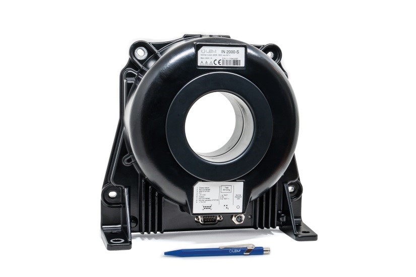
The complete transducer is shown in figure 8. The housing is metallic to give best shielding from external sources of interference. EMC immunity is further improved by situating the fluxgate inside the primary magnetic circuit.


Figure 8: The IN 2000 transducer


Table of key performance parameters.


The values of some important specification parameters of the IN 2000 are shown in Table 1.


Parameter Symbol Unit Maximum Value; -40 OC to 85 OC
Supply voltage UC Volts +/- 15, +/- 5%
Nominal current measuring range IPN A rms +/-2000 (IN 2000 transducer); AC and DC
Total current measuring range IPM A +/- 3000 Amps
Number of secondary turns Ncomp 2000
Output RMS noise up to 10 Hz, 10 kHz, 160 kHz Ino ppm 0.1, 4, 10 respectively
Output peak-to-peak ripple at 16 kHz Ino pp ppm 50
Offset at output IOE ppm +/- 10
Temperature coefficient of IOE TCIOE ppm/K 0.1
Linearity error over total measuring range eL ppm < 3
Step response time to 90% of IPN tr ms < 1
Frequency bandwidth (-3dB) BW kHz 140

Table 1: Some performance parameters. All values expressed as ppm are relative to the total current measuring range.


Characterization results.


An extensive characterization of the IN 2000 has been performed over the full temperature range. As an example, figure 9 shows the accuracy of a population of parts both at -40 OC and at 85 OC.


Figure 9. Characterization of the IN 2000 thermal drift compared with 25 OC at cold and hot extremes of temperature.


Conclusion


In general the validation of apparatus and equipment is made by certified laboratories using high-performance test benches supported by high-technology measuring devices including extremely accurate current transducers. These must therefore maintain their accuracy over the full temperature range of the equipment tested, for example, in automotive tests benches.

Performance which is needed for test equipment is also desirable for traditional industrial applications which are more and more demanding in high-performance applications such as medical equipment (e.g. MRI, proton therapy etc.), precision motor controllers and metering.

The IN 2000 transducer represents a new step forward in the performance which may be obtained from fluxgate transducers. Its high accuracy and low noise, both maintained over a wide temperature range, together with its compact physical size, will increase the breadth of applications for which this type of current transducer is the optimum choice.

img-capa-artigo-amds4-lower-size

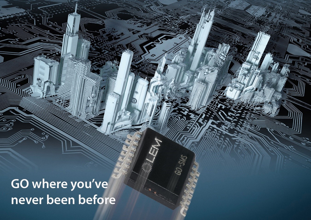
Come discover more about the new miniature sensor – GO Series

A New Family of Miniature, Fast and Accurate Transducers for Isolated Current Measurement


David Jobling; David Barbagallo; Julien Feignon

LEM International SA

Plan-les-Ouates, Geneva, Switzerland


Abstract:


The design of isolated current transducers has been continuously driven by cost and size reduction. Continuing this trend, a new family of transducers needing no magnetic circuit has been introduced in standard small-outline integrated circuit packages. Careful design results in their accuracy being similar to those of conventional transducers with only a modest reduction in isolation voltage. Some extra features have been added.


Introduction:


Current transducers in which isolation is required generally detect the magnetic field of the measured current; this has the additional advantage of allowing both AC and DC currents to be measured. There have been two aspects to the trend in LEM open-loop current transducers in recent years: cost and size have been continuously reduced, and by using custom proprietary CMOS ASICs as the sensing element the performance parameters such as accuracy and response time approach those of more complex closed-loop transducers (Ref 1). Usually the ASIC is placed in the air gap of a small magnetic circuit which gives noise-free amplification of the field and screening from external interference. Most of LEM’s conventional open loop transducers measure currents in the range of 10 A to 100’s of A, isolation levels are up to 8 kV and the response time from 2 us.


Some applications, particularly for motor drives, have the same need for speed but are less demanding of the current range and isolation levels while having strong pressure on price. In applications such as for example white-goods, window shutters and air-conditioning low cost and small size are particularly important. For these cases LEM has now introduced an additional family of sensors, the “GO” family, whose size is reduced even further by eliminating the magnetic circuit. Instead, the primary current is passed directly into a standard integrated circuit package where its magnetic field is measured by a new ASIC derived from that used in conventional transducers. Figure 1 shows two such examples. One is in an SOIC-8 package and the 4 secondary-side pins are for the supplies, the output voltage Vout and a reference voltage Vref. The other is in an SOIC-16 package where 8 secondary pins are available so the opportunity has been taken to provide two different Over-Current Detect (OCD) warning levels; one very fast, and the other slower but more accurate. The speed and accuracy of the GO transducers are very similar to those of a transducer with a magnetic circuit. The absence of a magnetic circuit of course means that there is zero magnetic offset.


Figure 1: The GO series transducers and their pin connections in SOIC-8 and SOIC-16 packages.


Architecture and features:


The GO transducer ASIC is derived from that used in LEM open-loop transducers which have a magnetic circuit. There is considerable production experience with this ASIC, which has allowed introduction of some extra features around the well-known signal path blocks. In this section the design of the GO transducer is described and some contrasts are made with magnetic circuit transducers.


Figure 2: Block diagram of a GO transducer in an SOIC-16 package.


Figure 2 shows a simplified block diagram of a GO transducer in a 16-pin package. Multiple Hall cells implanted in the ASIC are placed on both sides of the primary current to detect its magnetic field. Their offset, together with that of the input amplifiers, is eliminated with chopping techniques which modulate the Hall cell output to an AC signal. After amplification the Hall signal is demodulated back to its original frequency before buffering and filtering at the output. The fast response time is achieved by using a high chopping frequency and internal filters which reduce the noise bandwidth of the system.


During production each transducer is individually calibrated. Tests are done at 3 temperatures; the drifts of sensitivity and output offset are measured and corrections stored in an EEPROM memory on the ASIC; this ensures that the transducer accuracy is maintained over temperature and aging.


The ASIC is separated from the primary conductor by a series of insulating layers – an optimum separation has been chosen for the best compromise between highest isolation with a wide separation and highest magnetic field at the Hall cells with lower separation. The Hall cells on opposite sides of the primary are sensitive to fields in opposite directions so the transducer is immune to uniform magnetic fields from sources other than the measured current. The exact lateral position of the Hall cells relative to the primary is not critical, since the difference between the outputs of the cells on the opposite sides is used. In other words, the Hall cells are configured as a gradient sensor.


Figure 3: Block diagram of the Over-Current Detect (OCD) systems.


The detail of the OCD implementation is shown in figure 3. The aim is to give two different levels of warning. The first level is for currents slightly higher than expected, to warn for example that a drive current is going out of the expected range. This OCD needs to be reasonably accurate, not especially fast, and each user may want to set a different level. The relaxed speed requirement allows the input to this first OCD to be taken from the transducer output, and the level is set by user-chosen external resistors, hence its name, OCD_EXT.


The second level is intended to warn of currents which are dangerously high, due to a short circuit for example. The response time must be extremely fast, but the value and accuracy of the of the detection level are not critical. To obtain a fast response time and to allow an OCD level outside the normal linear operating range the input to the second OCD is taken before the demodulation block. Its level is set internally by storing a parameter internally in the EEPROM – so it is known as OCD_INT. The level is typically set at 3x the nominal primary current, IPN.


Figure 3 is slightly simplified: it omits the detail that ensures that both OCDs respond to both positive and negative over-currents.


Both OCDs check that the over-current condition is present for at least 1us approximately, to avoid false alarms, and both outputs, once triggered, are maintained for 10us to be sure that the condition can be detected. The outputs are open-drain, which conveniently allows OCDs from several transducers to be connected together. OCD_INT triggers in less than 2.1 us; the typical response time of OCD_EXT is 10 us.


The footprint of a GO series transducer in a 16-pin package is about 100 mm2, and in an 8-pin package it is half of this. The corresponding value for the smallest PCB-mounted transducer with a magnetic circuit is about 400 mm2. The heights are 2.5 mm and 12 mm respectively. However, for both types, in the higher current ranges some allowance must be made for dissipation of the heat generated in the transducer primary, which is greater in the GO series since the primary resistance is higher.


Key parameters and measured transducer performance


In Table 1 some of the key electrical parameters of the GO series transducers are presented. For comparison, the values of the same parameters for a small open-loop transducer with a magnetic circuit are also given – a small transducer has been chosen to give the most meaningful comparison, a larger transducer would have different parameter values.


Parameter GO transducers Magnetic circuit based transducers
 
Nominal current range 10 A – 30 A 3 A – 50 A
Supply 3.3 V or 5 V; 19 mA 3.3 V or 5 V; 19 mA
External field immunity Yes: gradient sensor Yes: magnetic circuit screen
Insulation test, 50 Hz, 1 min 3 kV 4.3 kV
Impulse test voltage, 50 us 4 kV 8 kV
Creepage, clearance distances SOIC-8: 4 mm; SOIC-16: 7 mm >8 mm
Accuracy at 25°C 1.0% 1.0%
Accuracy over 25 – 105°C 3.0% 3.4%
Primary resistance 0.7 mW 0.2 mW
Out-of-range detection Yes, 10 us response time No
Short-circuit detection Yes, 2.1 us response time Some models, 2.1 us
Response time <2.5 us <2.5 us
Offset drift (10 A model) 0.9 mA/K 0.9 mA/K
Sensitivity drift 150 ppm/K 200 ppm/K
Magnetic offset 0 0.25 A after 10x IPN
Footprint 50 – 100 mm2 400 mm2 or more
Height 2.5 mm 12 mm or more

Table 1: Comparison of key parameters of GO series and magnetic circuit based transducers.


Table 1 shows that many key electrical parameters have been inherited unchanged or slightly improved from the established sensors with a magnetic circuit, whereas others, such as size and insulation, are different, allowing the two transducer families to address quite different markets.


Figure 4: Response time measurement of a GO transducer.


Figure 4 shows a measured response time after a primary current change in 0.3 us. The compact size and absence of magnetic components in the transducer gives a response with very little overshoot and ringing.


The assertion made previously that the GO transducers are not disturbed by external magnetic field will be true if the amplified electrical output of the Hall cells from both sides is the same, since the difference between the two outputs is used. To satisfy this condition:


(i) The sensitivity of the Hall cells on both sides of the primary (and the amplifiers to which they are connected) must be the same; that is, they must be well matched;

(ii) The magnetic field must be the same on both sides of the primary; it must be uniform.


Considering point (i), because the Hall cells and the amplifiers are made with large devices, their matching is excellent. When a uniform external magnetic field is applied to a GO transducer it is almost perfectly rejected.


However, for point (ii) the magnetic fields generated by conductors placed close to the transducer are not uniform and the outputs from the two sides of the primary will not be perfectly rejected. This has been investigated for conductors placed in 4 different positions near a GO transducer; see figure 5. The worst case is position 3 in which the external conductor is aligned with the GO primary. If the external conductor carries 10 A and the measured current is also 10 A the transducer output error due to the external current will be only about 1% of the measured current even with zero distance between the external conductor and the GO. This investigation shows that with a minimum of care in the design of PCB layout, external conductors will have negligible influence on the accuracy of GO series transducers.


Figure 5: The effect of external conductors on the accuracy of a GO transducer. The error is shown when the currents in the GO primary and the external conductor are the same.


Another important consideration in miniature transducers is the effect of a sudden primary voltage change on the transducer output. This is best handled at the ASIC level. Where internal signal levels are small they are always differential, and changes in their common mode level due to an external transient have little effect. Sensitive nodes can be protected by small grounded screens on the top metal layer. Screening is used only over the small areas where it is needed. This has many advantages over large screens: the top metal layer remains available for interconnect where screens are not needed; the ASIC die is not hidden and damaged parts can be analysed, and there are no Eddy currents which would slow the response time.


Figure 6 shows the effect of a dv/dt of 5kV/us on the output of a 25 A GO (GO 25-SMS). The peak disturbance on the output is 4% of IPN and the recovery time is about 3.6 us.


Figure 6. Response of a GO transducer (GO 25-SMS) after a dv/dt disturbance.


Conclusion


This paper has introduced a new series of miniature, fast and accurate transducers for isolated measurement of AC and DC currents. Some of their electrical parameters are similar to those of transducers with magnetic circuits and others are altered. Different transducers will be suited to different applications and the addition of this series to the LEM catalogue will extend system designers’ possibilities for optimizing their systems with the most efficient cost effective means of isolated current measurement.


Reference 1: David Jobling: New open-loop current transducers with near closed-loop performance. Proceedings of the PCIM Conference, May 2014, page 222-6.

img0-amds4-low

Lançamento da Família de Transdutor LZSR

A nova série de transdutor de corrente LZSR, da LEM, oferece uma faixa de medição de até 450 A pico, possuindo tecnologia por efeito hall de loop fechado.


Genebra, Suíça – 7 de maio de 2019 – LEM anuncia a família de transdutores LZSR, uma nova linha que pode ser montada em placas de circuito impresso (PCBs) para medições isoladas, não intrusivas de correntes CC, CA e pulsadas de 100A a 200A nominais. A família é composta inicialmente por três modelos: LZSR 100-P, LZSR 150-P e LZSR 200-P.

Esses novos transdutores são baseados na mais recente tecnologia de ponta, a ASIC da LEM, que foi comprovada na série de transdutores de corrente LF xx10, LH e LXSR, lançadas anteriormente. Usado no modo de loop fechado, o ASIC baseia-se na tecnologia de efeito Hall e pode atingir um baixo drift de offset de até 3 ppm /K de VREF. Esta nova série aproveita esses benefícios em modelos para correntes de 100, 150 e 200A nominal.

Trabalhando em uma faixa de temperatura de -40 °C a + 85 °C, o drift de offset do LZDR é muito melhor (até 7 vezes) do que a geração anterior de transdutores de corrente por efeito Hall de loop fechado, que utilizavam o chip de efeito Hall tradicional.

Operando com alimentação simples de + 5 V, os modelos do LZSR medem a corrente de pico até 3 vezes a corrente nominal primária, atingindo 450 A pico para 150 ARMS (LZSR 150-P/SP1). Eles fornecem sua tensão de referência interna no pino VREF.

Uma saída para detecção de sobrecorrente, com um limite definido em 1,93 x IPN, também é oferecida como uma opção padrão disponível em um pino adicional. Essa função pode dar uma indicação de que uma corrente medida está excedendo seu valor esperado ou pode desligar a energia no caso de um curto-circuito.

O LZSR vem para o mercado com tamanho muito compacto de 37,75 x 48,2 x 19,4 mm para cada faixa de corrente e sem comprometer o alto isolamento fornecido entre os circuitos primário e secundário.

Técnicas avançadas de fabricação inspiradas em projetos automotivos também foram introduzidas, permitindo que esses novos transdutores alcancem os mais altos níveis de qualidade.

Os modelos estão disponíveis com uma abertura para o condutor primário (LZSR-P) ou integrando o condutor primário a ser soldado na placa de circuito impresso (LZSR-TP).

Esta série será particularmente adequada para aplicações em que o baixo drift de offset é importante, como na geração mais recente de inversores solares de 70 a 120 kW (medição do lado CA), em que os padrões exigem uma baixa componente CC  na corrente de saída.

Cobertos pela garantia de cinco anos da LEM, os transdutores de corrente da série LZSR têm a marcação CE e estão em conformidade com os mais recentes padrões industriais.